Optical diode based on asymmetrical metal double-gate structure
A technology of optical diode and double grid structure, which is applied in the coupling direction of diffraction grating and optical waveguide to achieve the effect of simple structure
- Summary
- Abstract
- Description
- Claims
- Application Information
AI Technical Summary
Problems solved by technology
Method used
Image

Examples
Embodiment Construction
[0021] The embodiments of the present invention are described in detail below. This embodiment is implemented on the premise of the technical solution of the present invention, and detailed implementation methods and specific operating procedures are provided, but the protection scope of the present invention is not limited to the following implementation example.
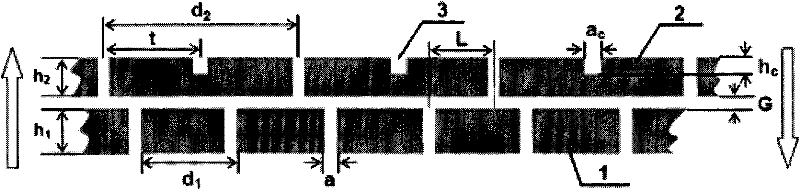
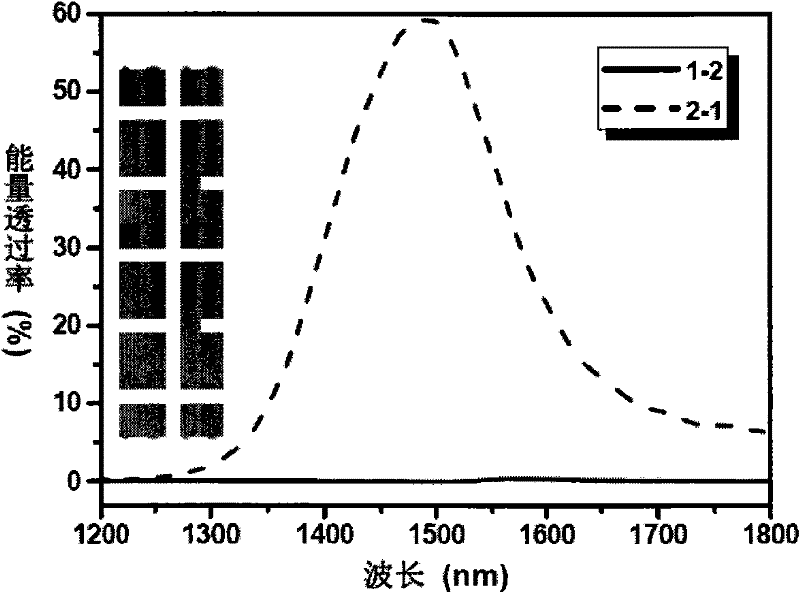
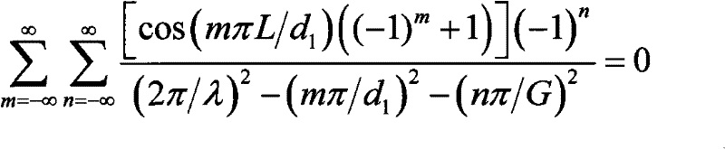
[0022] Such as figure 1 As shown, this embodiment includes a first metal grid 1 and a second metal grid 2, wherein: the grid period of the second metal grid 2 is twice that of the first metal grid 1, and the second metal grid 2 and the first metal grid 1 Arranged in parallel, surface microcavities 3 are provided on the outer surface of the second metal grid 2 . There is a gap G and a lateral displacement L between the first metal grid 1 and the second metal grid 2, which satisfy the transmission suppression relationship of the electromagnetic wave with a wavelength λ taking the first metal grid 1 as the incident e...
PUM
 Abstract
Description
Claims
Application Information
 - R&D
- Intellectual Property
- Life Sciences
- Materials
- Tech Scout
- Unparalleled Data Quality
- Higher Quality Content
- 60% Fewer Hallucinations
Browse by: Latest US Patents, China's latest patents, Technical Efficacy Thesaurus, Application Domain, Technology Topic, Popular Technical Reports.
© 2025 PatSnap. All rights reserved.Legal|Privacy policy|Modern Slavery Act Transparency Statement|Sitemap|About US| Contact US: help@patsnap.com