TFT-LCD (Thin Film Transistor-Liquid Crystal Display) array substrate

An array substrate and substrate technology, which is applied in the field of thin film transistor liquid crystal displays, can solve problems such as gate line disconnection or data line disconnection, gate line and data line short circuit, and many maintenance procedures, so as to reduce gate line disconnection or data and reduce area , Increase the effect of line redundancy

Active Publication Date: 2011-06-01
BOE TECH GRP CO LTD +1
View PDF0 Cites 4 Cited by
  • Summary
  • Abstract
  • Description
  • Claims
  • Application Information

AI Technical Summary

Problems solved by technology

[0005] The purpose of the present invention is to provide a TFT-LCD array substrate to effectively solve technical defects such as short circuit of gate line and data line, open circuit of gate line or open circuit of data line in the production of existing TFT-LCD array substrate, and further solve the problem of existing TFT-LCD array substrate. There are technical defects such as many technical maintenance procedures, long time, low success rate, etc.

Method used


Image

  • TFT-LCD (Thin Film Transistor-Liquid Crystal Display) array substrate
  • TFT-LCD (Thin Film Transistor-Liquid Crystal Display) array substrate
  • TFT-LCD (Thin Film Transistor-Liquid Crystal Display) array substrate

Examples


Embodiment Construction

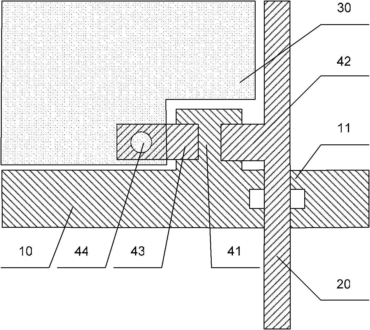
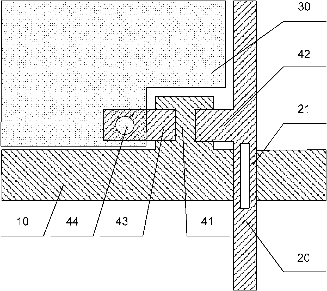
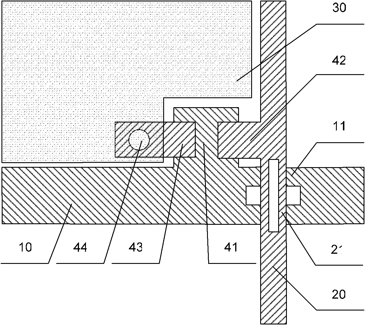
[0036] figure 1 It is a structural schematic diagram of the first embodiment of the TFT-LCD array substrate of the present invention. Such as figure 1As shown, the main structure of the TFT-LCD array substrate in this embodiment includes gate lines 10, data lines 20, pixel electrodes 30, and thin film transistors (TFTs) formed on the substrate, and the crossed gate lines 10 and data lines 20 define In the pixel area, the pixel electrode 30 is formed in the pixel area. Specifically, a thin film transistor as a switching device at least includes a gate electrode 41, a source electrode 42 and a drain electrode 43, the gate electrode 41 and the gate line 10 are located under the gate insulating layer, and the source electrode 42, the drain electrode 43 and the data line 20 are located under the gate electrode 41. On the insulating layer, a passivation layer is formed on it, and a passivation layer via hole 44 is formed at the position of the drain electrode 43, and the pixel e...


PUM


Abstract

The invention relates to a TFT-LCD (Thin Film Transistor-Liquid Crystal Display) array substrate. The TFT-LCD array substrate comprises grid lines, data lines, pixel electrodes and a thin film transistor which are formed on the substrate, wherein at the intersection of the grid lines and the data lines, the grid lines at both sides of the data lines are connected by a grid connecting line which forms a double-point or multi-point intersection structure with the data lines; the grid connecting line comprises at least two first grid connecting lines; and the first grid connecting lines and the grid lines are made of the same material and are positioned at the same layer. By arranging at least two first grid connecting lines to intersect the data lines at the intersection, the invention lowers the probability of short circuit failure of the grid lines, and lowers the probability of open circuit failure of the grid lines. Meanwhile, the TFT-LCD array substrate provided by the invention also has the advantages of simple repairing process, fewer procedures, short time, high maintenance success rate and the like when the grid lines are subjected to short circuit and open circuit failure.

Description

[0001] This application is a divisional application of the patent application No. 200710178944.8 (the filing date of the original application is December 7, 2007, and the name of the invention is TFT-LCD array substrate). technical field [0002] The invention relates to a thin film transistor liquid crystal display, in particular to a thin film transistor liquid crystal display array substrate. Background technique [0003] Thin Film Transistor Liquid Crystal Display (TFT-LCD for short) has the characteristics of small size, low power consumption, no radiation, and relatively low manufacturing cost, and occupies a dominant position in the current flat panel display market. TFT-LCD array substrate is one of the important parts of TFT-LCD, its structure is as follows Figure 12 As shown, it mainly includes a substrate as a substrate, a gate electrode 41 and a gate line 10 formed on the substrate, a gate insulating layer (not shown) formed on the gate electrode 41 and the gate ...

Claims


Application Information

Patent Timeline
Patent Type & Authority Applications(China)
IPC IPC(8): G02F1/1362G02F1/1368H01L27/02
Inventor 申伟权基瑛
Owner BOE TECH GRP CO LTD
Why Eureka
Try Eureka