TFT-LCD pixel structure
A technology of pixel structure and pixel area, applied in optics, instruments, electrical components, etc., can solve the problems of open circuit of the common electrode line, bad common electrode line, low maintenance success rate, etc., to improve the charging speed, reduce related defects, and respond quick effect
- Summary
- Abstract
- Description
- Claims
- Application Information
AI Technical Summary
Problems solved by technology
Method used
Image
Examples
Embodiment Construction
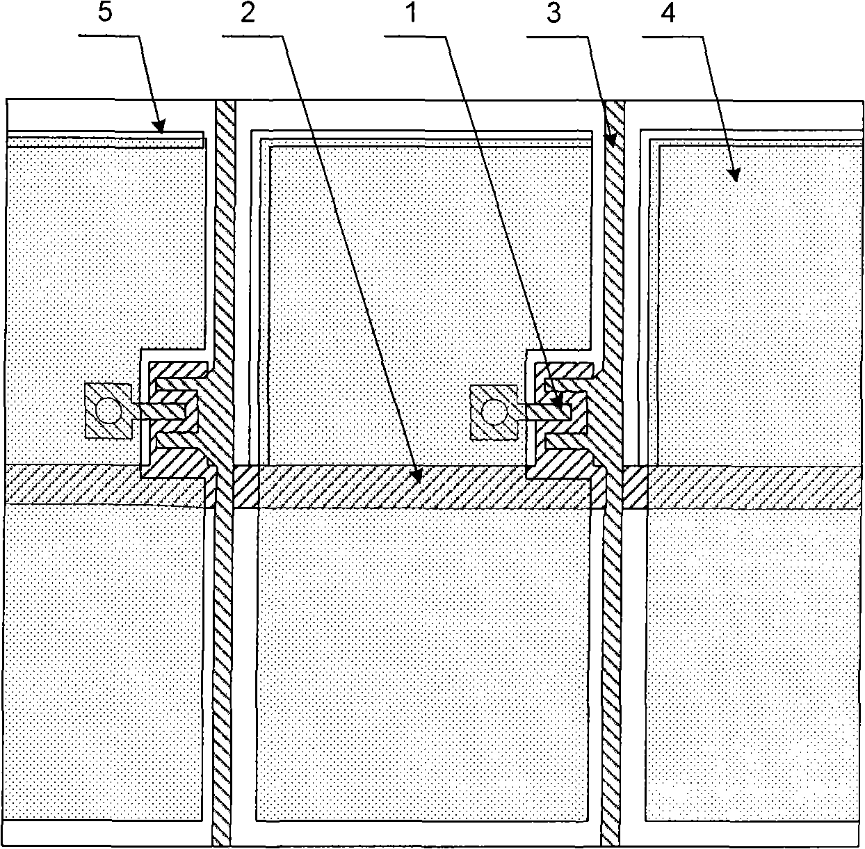
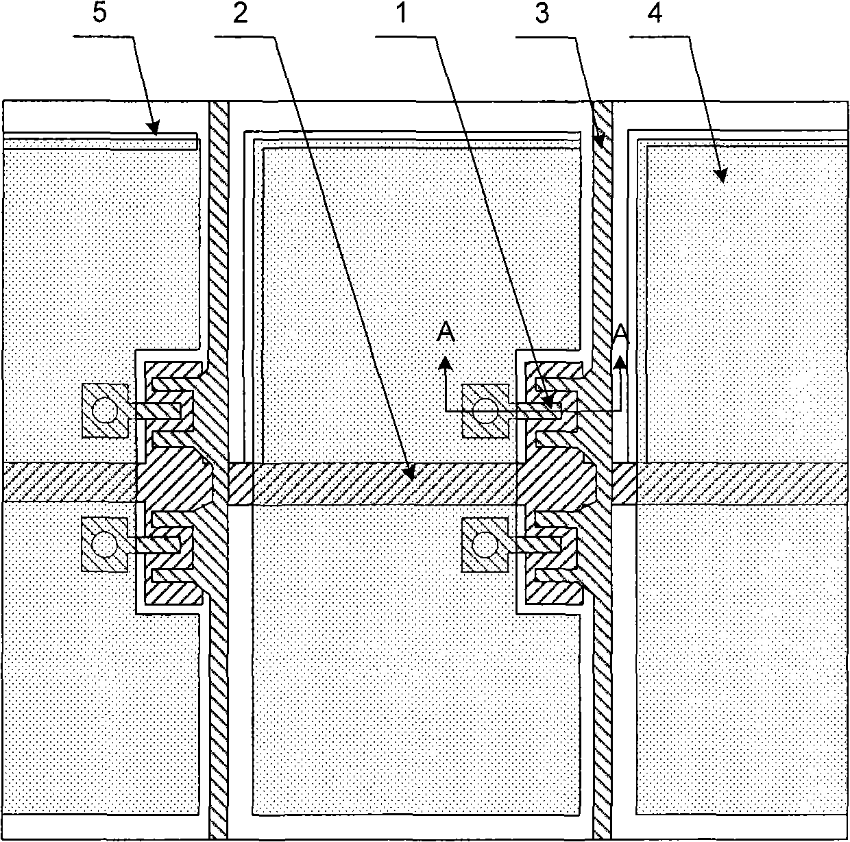
[0027] figure 1 It is a schematic structural diagram of the first embodiment of the TFT-LCD pixel structure of the present invention. Such as figure 1 As shown, the TFT-LCD pixel structure of this embodiment includes a thin film transistor 1, a gate line 2, a data line 3, and a pixel electrode 4. The gate line 2 is horizontally arranged in the middle of the pixel area, and the data line 3 is perpendicular to the gate line 2. Setting, located on one side of the pixel area (e.g. figure 1 The right side of the pixel area), the intersection of the gate line 2 and the data line 3 forms a thin film transistor 1. The thin film transistor 1 is connected to the pixel electrode 4 formed in the pixel area, and the gate line 2 and the pixel electrode 4 in the middle of the pixel area form a storage capacitance.
[0028] The above technical solution of this embodiment eliminates the common electrode line, and forms a storage capacitor from the gate line and the pixel electrode in the middl...
PUM
 Abstract
Description
Claims
Application Information


