

Organic light emitting diode (OLED) device
A device and organic material technology, applied in the field of OLED devices, can solve the problems of affecting device performance, short device service life, and reduced device efficiency, and achieve the effects of improving luminous efficiency, reducing easy aging, and improving device life.
- Summary
- Abstract
- Description
- Claims
- Application Information
AI Technical Summary
Problems solved by technology
Method used
Image

Examples
Embodiment Construction
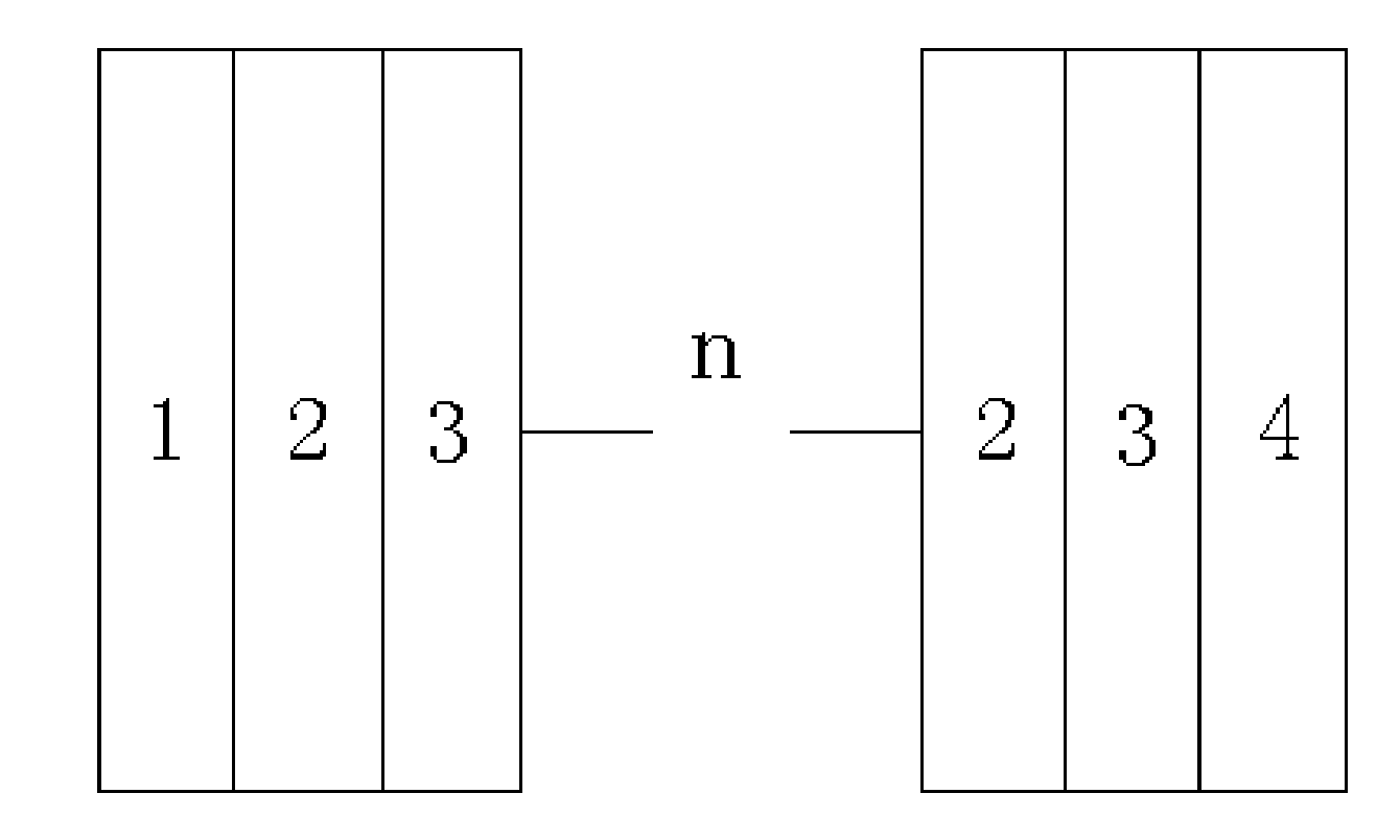
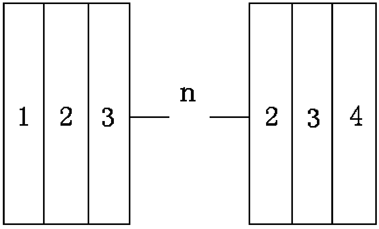
[0011] The OLED device of the present invention and its preparation method are described in detail below in conjunction with the structural diagram:
[0012] see figure 1 As shown, the OLED device of the present invention includes an anode 1 and a cathode 4, and an organic material 3 and a transition metal oxide 2 arranged between the anode 1 and the cathode 4, and the organic material 3 and the transition metal oxide group 2 form an n-dimensional quantum well structure. Wherein, the organic material 3 serves as a light-emitting layer and an electron transport layer, and the transition metal oxide 2 serves as a hole transport layer and an electron transport layer.
[0013] The n-dimensional quantum well structure is 1, 2, 3, or 4-dimensional. The metal oxide is molybdenum oxide MoO x , Tungsten Oxide WO 3 or vanadium pentoxide V 2 o 5 One of them, the thickness range is 5-60nm. Described organic material is Alq 3 (Tris(8-hydroxy-quinolinato)aluminium), AND(9,10-di(naph...
PUM
 Abstract
Description
Claims
Application Information