Medium slit optical waveguide
A technology of slit light and medium, applied in the field of optical waveguide, can solve problems such as weak confinement ability
- Summary
- Abstract
- Description
- Claims
- Application Information
AI Technical Summary
Problems solved by technology
Method used
Image

Examples
example
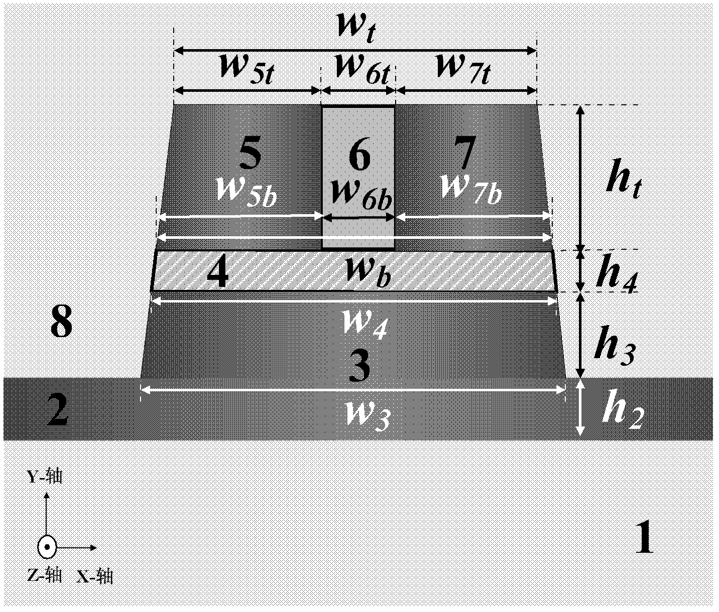
[0021] figure 2 It is the structural diagram of the dielectric slit optical waveguide described in the example. 201 is the base layer, n s Its refractive index; 202 is a high refractive index buffer layer, and its height is h b ; 203 is a high refractive index medium layer, its cross section is square, and its height is h 1 ; 204 is a low refractive index medium layer, its cross section is square, and its height is h l ; 205 and 207 are high-refractive index medium regions, and their cross-sections are square, w h Its width; 206 is the low emissivity medium area, its cross-section is square, n 1 is its refractive index, w s Its width; the heights of 205, 206, and 207 are equal and all are h 2 ; 205, 206, 207 jointly constitute the width of the cross section of the region, the width of 204, the width of 203 are equal, and both are w; the refractive index of 202, 203, 205, 207 is n h ; 208 is cladding, n c for its refractive index.
[0022] In this example, the wavelen...
PUM
 Abstract
Description
Claims
Application Information
 - R&D Engineer
- R&D Manager
- IP Professional
- Industry Leading Data Capabilities
- Powerful AI technology
- Patent DNA Extraction
Browse by: Latest US Patents, China's latest patents, Technical Efficacy Thesaurus, Application Domain, Technology Topic.
© 2024 PatSnap. All rights reserved.Legal|Privacy policy|Modern Slavery Act Transparency Statement|Sitemap