

Method for measuring ohmic contact resistivity between black silicon material and metal electrodes
A metal electrode, ohmic contact technology, applied in the direction of measuring resistance/reactance/impedance, measuring electrical variables, measuring devices, etc., can solve the problems of testing the specific contact resistivity of black silicon materials and metal electrodes, and achieve convenient specific contact resistivity. , to avoid parasitic resistance, the effect of high accuracy
- Summary
- Abstract
- Description
- Claims
- Application Information
AI Technical Summary
Problems solved by technology
Method used
Image

Examples
Embodiment Construction
[0035] In order to make the object, technical solution and advantages of the present invention clearer, the present invention will be further described in detail below in conjunction with specific embodiments and with reference to the accompanying drawings.
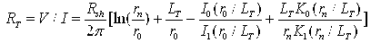
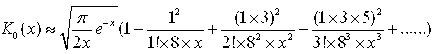
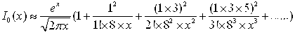
[0036] Because the present invention needs to quote the dot-shaped transmission line model method to test the specific contact resistivity between the black silicon material and the metal electrode, below in conjunction with the test circuit structure provided by the present invention, the operating principle of the dot-shaped transmission line model method is necessary instruction of.
[0037] Such as figure 1 As shown, at first, at least 6 dot-shaped contact electrodes (such as figure 1 , 2 , 3, 4, 5, and 6), each dot-shaped electrode consists of a radius r 0 The inner contact circle and an outer contact circle whose inner diameter gradually increases, where the inner diameter of the outer contact circle is r n , an...
PUM
| Property | Measurement | Unit |
|---|---|---|
| size | aaaaa | aaaaa |
Abstract
Description
Claims
Application Information