Semiconductor substrate dicing device and semiconductor wafer dicing manufacturing method
A manufacturing method and semiconductor technology, applied in semiconductor/solid-state device manufacturing, electrical components, circuits, etc., can solve problems affecting product yield and other issues
- Summary
- Abstract
- Description
- Claims
- Application Information
AI Technical Summary
Problems solved by technology
Method used
Image

Examples
Embodiment Construction
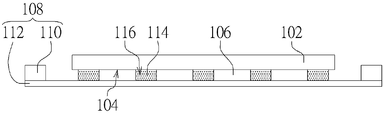
[0014] Please refer to figure 1 , Which illustrates a semiconductor wafer cutting device in a manufacturing method according to an embodiment. The semiconductor substrate 102 has a surface 104. Several dies 106 separated from each other are arranged on the surface 104 of the semiconductor substrate 102 and located between the semiconductor substrate 102 and the carrier 108. In one embodiment, the carrier 108 is, but is not limited to, a film frame, which may include an adhesive tape 112 supported by the frame 110.
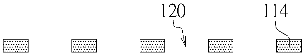
[0015] In an embodiment, the supporting element 114 fills the void 116 in the area on the surface 104 of the semiconductor substrate 102 where the die 106 is not provided. The position of the gap 116 may correspond to (including) the cutting lane. Therefore, in the step of dicing the semiconductor substrate 102, the semiconductor substrate 102 and the die 106 on it can be firmly fixed on the dicing tape 112 without shaking and abrasion to the dicing knife, and also ...
PUM
 Abstract
Description
Claims
Application Information
 - R&D
- Intellectual Property
- Life Sciences
- Materials
- Tech Scout
- Unparalleled Data Quality
- Higher Quality Content
- 60% Fewer Hallucinations
Browse by: Latest US Patents, China's latest patents, Technical Efficacy Thesaurus, Application Domain, Technology Topic, Popular Technical Reports.
© 2025 PatSnap. All rights reserved.Legal|Privacy policy|Modern Slavery Act Transparency Statement|Sitemap|About US| Contact US: help@patsnap.com