Flat pin chip tester

A test device and pin technology, which is applied in the direction of measuring device, electronic circuit testing, measuring electricity, etc., can solve the problems of unreliable connection performance, small contact surface, wear and so on.

Inactive Publication Date: 2016-06-15
ANTARES ADVANCED TEST TECH SUZHOU CO LTD
View PDF6 Cites 1 Cited by
  • Summary
  • Abstract
  • Description
  • Claims
  • Application Information

AI Technical Summary

Problems solved by technology

[0004] However, due to the point contact between the traditional spring probe and the pin of the chip under test, the contact surface is extremely small, and the connection performance is unreliable; large, which affects the test environment; moreover, the point contact method requires extremely high positioning accuracy of the tested chip, test circuit board, and spring probe; Pressing the contact, there must be wear and tear between the two, shortening the service life

Method used


Image

  • Flat pin chip tester
  • Flat pin chip tester
  • Flat pin chip tester

Examples


Embodiment Construction

[0019] The following will clearly and completely describe the technical solutions in the embodiments of the present invention with reference to the accompanying drawings in the embodiments of the present invention. Obviously, the described embodiments are only some, not all, embodiments of the present invention. Based on the embodiments of the present invention, all other embodiments obtained by persons of ordinary skill in the art without making creative efforts belong to the protection scope of the present invention.

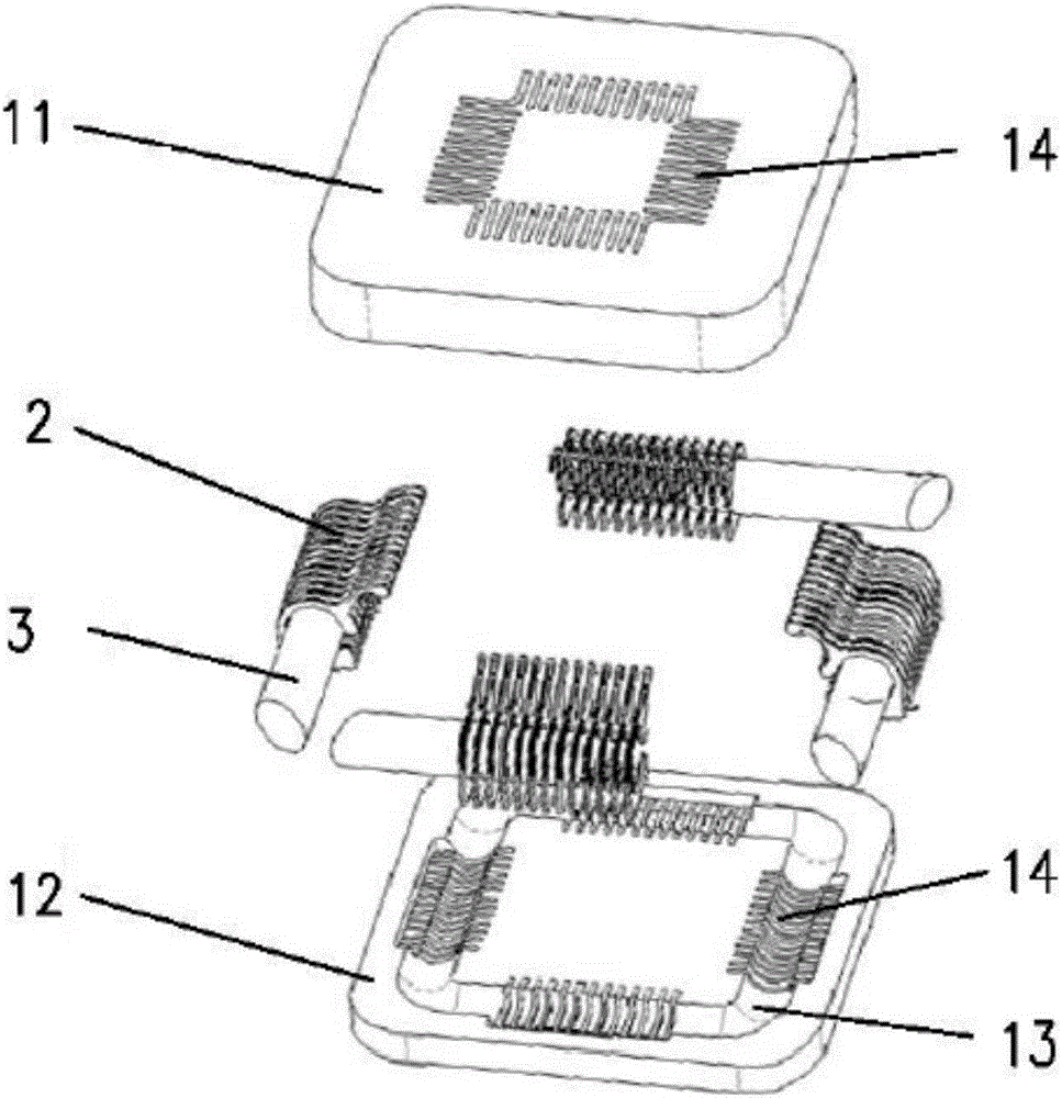
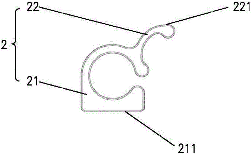
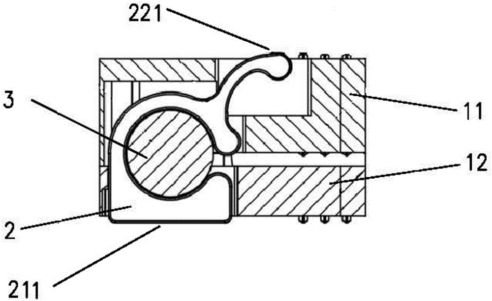
[0020] like Figure 1 to Figure 2 Shown, a kind of test device for flat pin chip, comprises test seat 1, insulating elastic rod 3 and several elastic conductive contact pieces 2 that are arranged side by side in multiple rows; The insulating elastic rod 3 is sandwiched in the test seat 1; the bottom outer edge of the elastic conductive contact piece 2 forms a lower contact surface 211 that is in line / surface contact with the test circuit board 5, and the top o...


PUM


Abstract

The invention discloses a flat pin chip tester, comprising a test seat, an insulation elastic rod and a plurality of parallel rows of elastic conductive contact pieces; the elastic conductive contact pieces parallel in a same row sleeve the insulation elastic rod and are clamped in the test seat; the bottom of the elastic conductive contact pieces forms a lower contact surface in contact with the line / surface of a test circuit board, and the top forms an upper contact surface in contact with the pin line of the chip to be tested; the upper contact surface and the lower contact surface respectively extend out of the upper surface and the lower surface of the test seat. According to the invention, the elastic conductive contact pieces are skillfully set to sleeve the insulation elastic rod and to be clamped in the test seat; a flat pin chip is tested in a line / surface contact mode, thereby overcoming the problems of unreliable performance, easy abrasion, great influence to test environment and poor compatibility caused by employing a spring probe to test in a point contact mode in the prior art.

Description

technical field [0001] The invention relates to the technical field of chip testing, in particular to a testing device for flat pin chips. Background technique [0002] In the semiconductor manufacturing industry, semiconductor chips need to be tested for electrical performance to check whether the chip meets the requirements of electrical performance. [0003] In the process of chip testing, the current and signal need to be connected and transmitted between the chip and the test circuit board through electronic connectors. The chip test socket is an indispensable connection test device in the entire test system. The traditional chip test socket includes The chip positioning plate made of high-strength composite insulating material, the main body of the test socket, the probe holding plate and the spring probe made of high-conductivity metal material. To put it simply, the spring probe is fixed by the main body of the test socket and the probe holding plate, so that one en...

Claims


Application Information

Patent Timeline
Patent Type & Authority Applications(China)
IPC IPC(8): G01R31/28
CPCG01R31/2831
Inventor 俞璟峰殷德骏张龙
Owner ANTARES ADVANCED TEST TECH SUZHOU CO LTD
Why Eureka
Try Eureka