Display device, array substrate and driving method thereof

A technology of array substrates and data-driven circuits, applied in static indicators, instruments, etc., can solve problems such as open circuit of data lines 11 and short circuit of data lines 11, and achieve the effect of reducing the arrangement density and avoiding short circuits or open circuits

Active Publication Date: 2016-08-31
XIAMEN TIANMA MICRO ELECTRONICS +1
View PDF7 Cites 26 Cited by
  • Summary
  • Abstract
  • Description
  • Claims
  • Application Information

AI Technical Summary

Problems solved by technology

However, as the resolution of the display device increases, the number of pixel units 12 increases, and the number of corresponding data lines 11 also increases. In the transition area A between the driving circuit 14 and the pixel units 12, the data lines 11 are arranged Dense, easy to cause short circuit of data line 11 or disconnection of data line 11

Method used


Image

  • Display device, array substrate and driving method thereof
  • Display device, array substrate and driving method thereof
  • Display device, array substrate and driving method thereof

Examples


Embodiment Construction

[0028] The following will clearly and completely describe the technical solutions in the embodiments of the present invention with reference to the accompanying drawings in the embodiments of the present invention. Obviously, the described embodiments are only some, not all, embodiments of the present invention. Based on the embodiments of the present invention, all other embodiments obtained by persons of ordinary skill in the art without making creative efforts belong to the protection scope of the present invention.

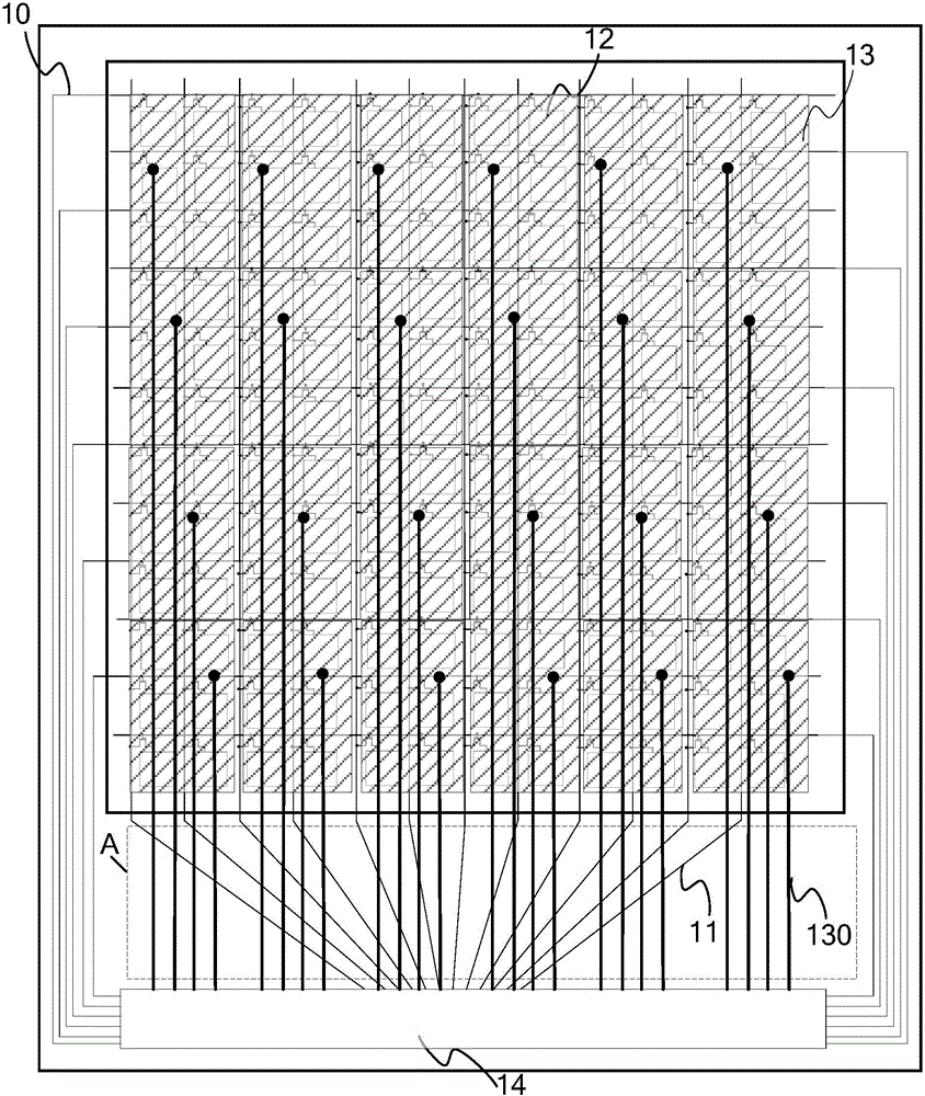
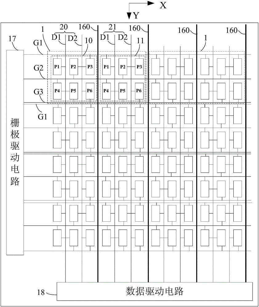
[0029] An embodiment of the present invention provides an array substrate, such as figure 2 as shown, figure 2 is a schematic top view of the array substrate. The array substrate includes a display area and a non-display area located around the display area. Wherein, the display area has a plurality of pixel groups 1 arranged in an array, that is, the plurality of pixel groups 1 are arranged in sequence along the row direction X, and the plurality of pixel...


PUM


Abstract

The invention provides a display device, an array substrate and a driving method thereof. Sub pixels from a first to a sixth in a each pixel unit in the array substrate are arranged in a two-row three-column mode; a first gate line in each gate line group is connected with the first sub pixel and the third sub pixel; a second gate line is connected with the second sub pixel and the fourth sub pixel; a third gate line is connected with the fifth sub pixel and the sixth sub pixel; a first data line in a first sub data line group is connected with the first sub pixel, the fourth sub pixel and the fifth sub pixel; and a second data line is connected with the second sub pixel, the third sub pixel and the sixth sub pixel. In comparison with the prior art, one data line is reduced for each three columns of sub pixels, the arrangement density of the data lines in a transition region can thus be reduced, and short circuit or broken circuit of the data lines can be avoided.

Description

technical field [0001] The present invention relates to the field of display technology, and more specifically, to a display device, an array substrate and a driving method thereof. Background technique [0002] Array substrates of existing display devices, such as figure 1 as shown, figure 1 is a schematic top view structure of the array substrate, the array substrate includes a plurality of gate lines 10, a plurality of data lines 11, a plurality of pixel units 12 and a plurality of touch electrodes 13, wherein each gate line 10 is connected with a driving The circuit 14 is electrically connected to provide a scan signal to its corresponding pixel unit 12; each data line 11 is electrically connected to the drive circuit 14 to provide a data signal to its corresponding pixel unit 12; each touch electrode 13 covers multiple Each touch electrode 13 is electrically connected to the drive circuit 14 through a touch lead 130 to provide a common voltage signal during the displa...

Claims


Application Information

Patent Timeline
Patent Type & Authority Applications(China)
IPC IPC(8): G09G3/20
CPCG09G3/20
Inventor 苏凌志赖青俊
Owner XIAMEN TIANMA MICRO ELECTRONICS
Why Eureka
Try Eureka