

Key node extraction method based on gate-level circuit simulation
A technology of gate-level circuits and key nodes, which is applied in the field of key node extraction of gate-level circuits, can solve problems such as high repetition rate, large search space, and high algorithm complexity, so as to speed up the recovery process, avoid repeated recovery, and improve search efficiency. efficiency effect
- Summary
- Abstract
- Description
- Claims
- Application Information
AI Technical Summary
Problems solved by technology
Method used
Image

Examples
Embodiment Construction
[0026] In order to make the object, technical solution and advantages of the present invention more clear, the present invention will be further described in detail below with reference to the accompanying drawings and examples.
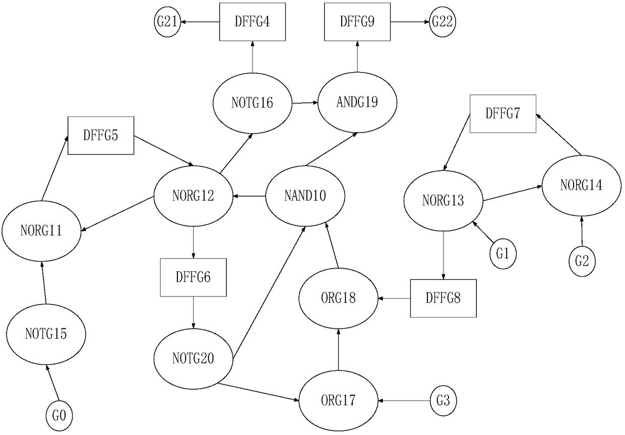
[0027] refer to figure 1 , the gate-level circuit targeted by the present invention includes 4 external input terminals G0, G1, G2, G3, 6 D flip-flops DFF nodes DFFG4, DFFG5, DFFG6, DFFG7, DFFG8, DFFG9, 3 NOT gates NOT nodes NOTG15, NOTG16, NOTG20, 1 AND node ANDG19, 2 OR nodes ORG17, ORG18, 4 NOR nodes NORG11, NORG12, NORG13, NORG14, 1 NAND node NANDG10 and 2 external outputs G21 , G22.
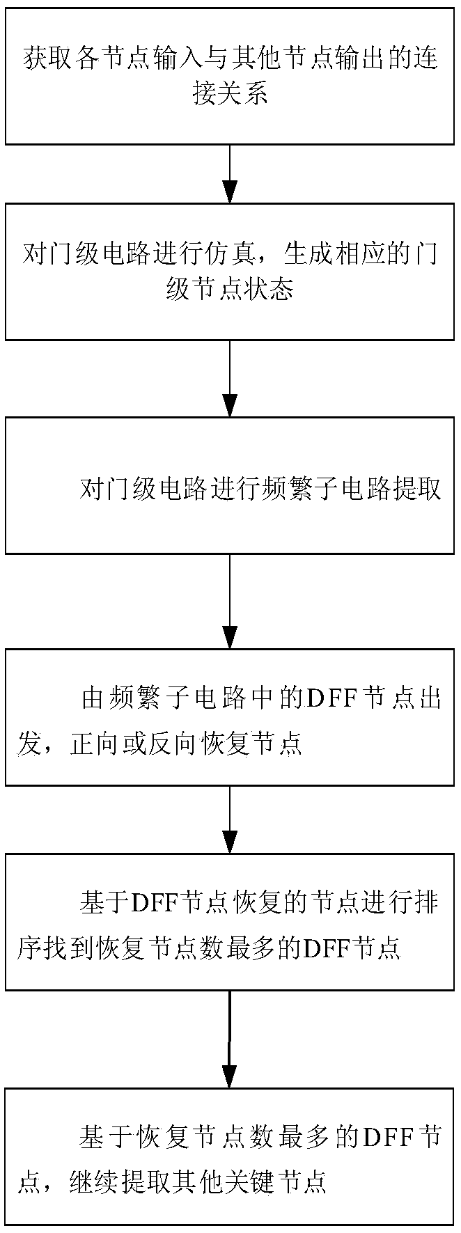
[0028] refer to figure 2 , the present invention is based on the key node extraction method of gate-level circuit simulation, comprises the following steps:
[0029] Step 1: Obtain the connection relationship of nodes in the gate-level circuit, and obtain the internal connection relationship of the gate-level circuit.
[0030] (1a) storing the gate-level circu...
PUM
 Abstract
Description
Claims
Application Information