

Array substrate, liquid crystal display panel and method for manufacturing array substrate
An array substrate and substrate technology, applied in the field of display screen, can solve problems such as hillock bulge, electrostatic discharge breakdown, tip power generation, etc.
- Summary
- Abstract
- Description
- Claims
- Application Information
AI Technical Summary
Problems solved by technology
Method used
Image


Examples
Embodiment Construction
[0024] The following will clearly and completely describe the technical solutions in the embodiments of the present invention with reference to the accompanying drawings in the embodiments of the present invention. Obviously, the described embodiments are only some, not all, embodiments of the present invention. Based on the embodiments of the present invention, all other embodiments obtained by persons of ordinary skill in the art without making creative efforts belong to the protection scope of the present invention. The patterned patterning process described in this application includes patterning processes such as film formation, development, exposure, and etching.
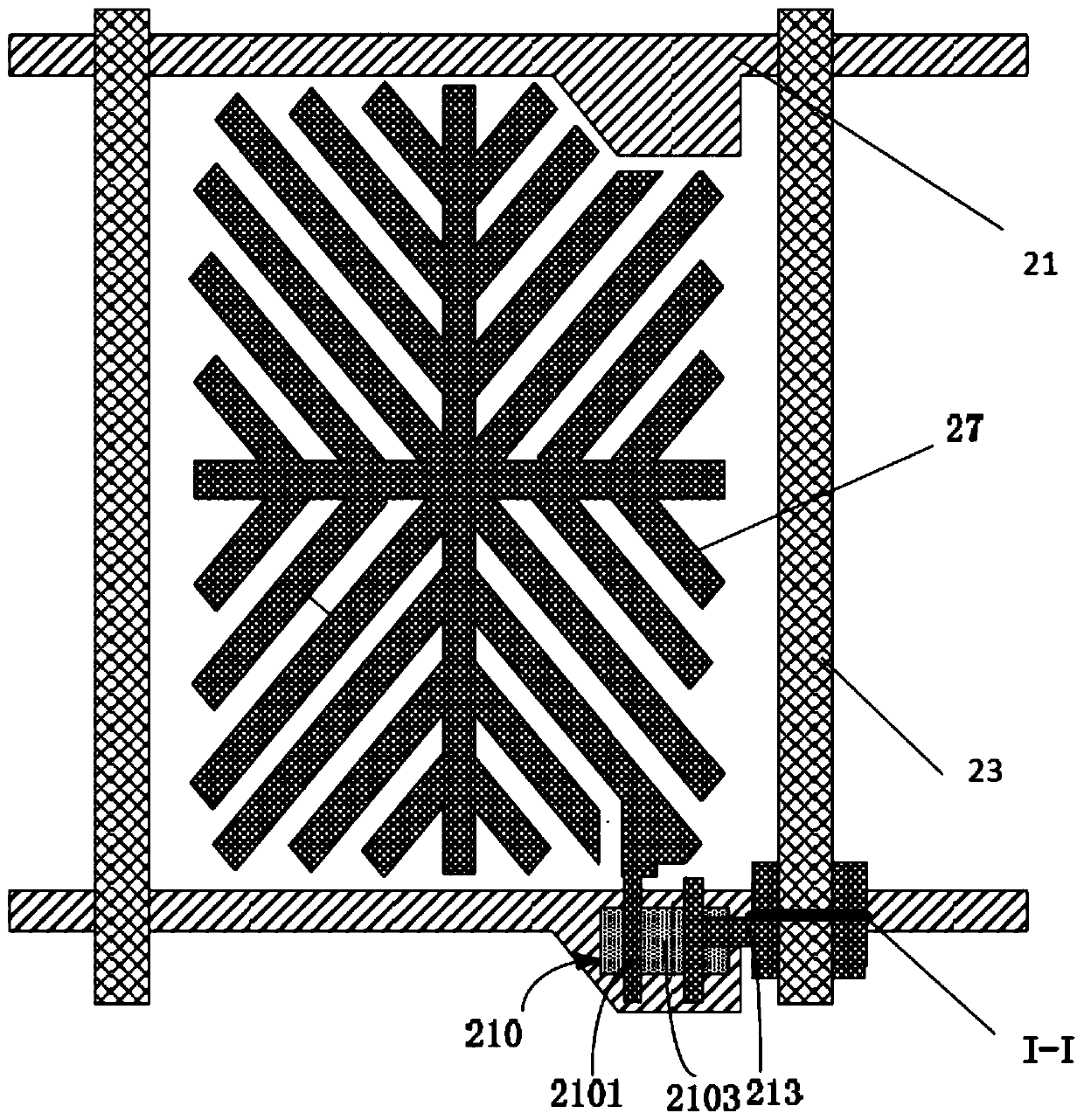
[0025] see figure 1 and figure 2 The present application provides an array substrate, which mainly refers to a low temperature polysilicon (LTPS) thin film transistor liquid crystal array substrate, which includes a first metal layer 211 formed on the substrate 10, an insulating layer 212, and a TFT switch 2...
PUM
 Abstract
Description
Claims
Application Information