Organic light emitting diode touch display substrate and touch display device

A technology for touch display substrates and light emitting diodes, applied in the fields of instruments, computing, electrical digital data processing, etc., can solve the problems of insufficient exposure of photoresist, short circuit of touch traces 06, low yield rate, etc., to improve short circuit phenomenon, the effect of improving product yield

Active Publication Date: 2020-05-12
SHANGHAI TIANMA MICRO ELECTRONICS CO LTD
View PDF6 Cites 0 Cited by
  • Summary
  • Abstract
  • Description
  • Claims
  • Application Information

AI Technical Summary

Problems solved by technology

The inventors of the present application found in the process of implementing the application that due to the structural characteristics of the dam, a depression with a large step difference will be formed between the inner dam and the outer dam. When connecting wire 06, short circuit between touch wires 06 is often caused due to insufficient exposure of the photoresist in the recess, such as Figure 1b S, which affects the realization of the touch display function of the product, and the yield rate is low

Method used


Image

  • Organic light emitting diode touch display substrate and touch display device
  • Organic light emitting diode touch display substrate and touch display device
  • Organic light emitting diode touch display substrate and touch display device

Examples


Embodiment Construction

[0034] In order to improve the short circuit phenomenon of the touch traces of the OLED touch display substrate and improve the product yield, the embodiments of the present invention provide an OLED touch display substrate and an OLED touch display device. In order to make the purpose, technical solution and advantages of the present invention clearer, the following examples are given to further describe the present invention in detail.

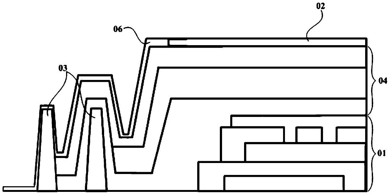
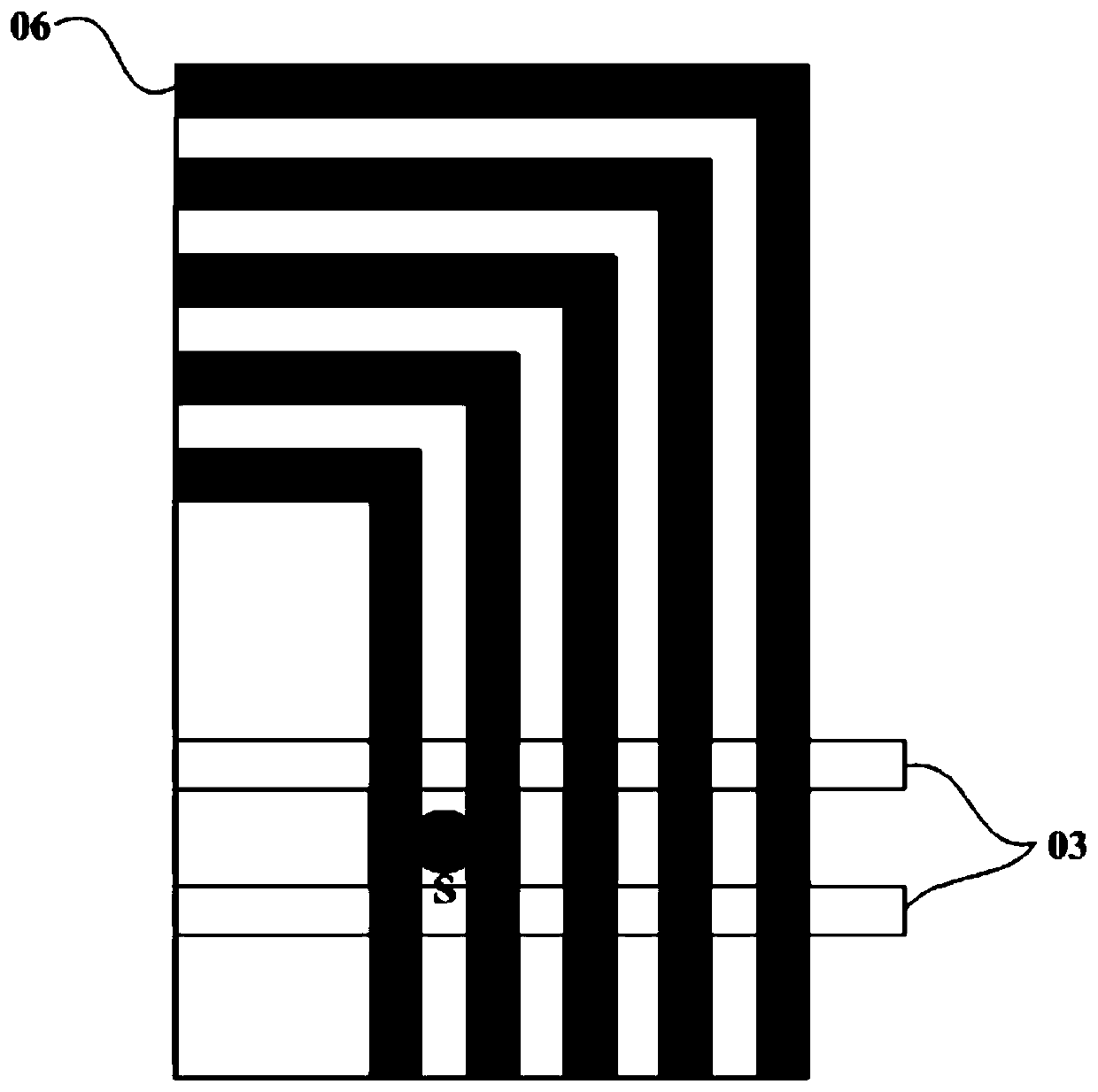
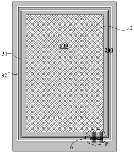
[0035] like figure 2 , Figure 3a ~ Figure 3d As shown, the OLED touch display substrate provided by the embodiment of the present invention includes a display area 100 and a peripheral area 200 surrounding the display area 100, wherein: the display area 100 includes an OLED display device 1 (see Figure 5 ) and the touch electrode part 2; the peripheral area 200 includes at least two circles of dams, the at least two circles of dams include a first dam 31 and a second dam 32, the first dam 31 is arranged around the display area 100, and t...


PUM


Abstract

The invention discloses an OLED (Organic Light Emitting Diode) touch display substrate and an OLED touch display device to eliminate a touch routing short circuit phenomenon and improve a product yield. The OLED touch display substrate comprises a display area and a peripheral area which surrounds the display area, wherein the display area comprises an OLED display device and a touch electrode part; and the peripheral area comprises at least two circles of box dams, wherein the at least two circles of box dams comprise a first box dam and a second box dam, the first box dam is arranged around the display area, and the second box dam is arranged around the first box dam. The OLED touch display substrate also comprises a film packaging layer, a plurality of separators and a plurality of touch routes, wherein the film packaging layer covers the OLED display device and is expanded to at least cover the first box dam; the plurality of separators are positioned between the first box dam and the second box dam and are arranged at intervals along a groove between the first box dam and the second box dam; and the plurality of touch routes are connected with the touch electrode part, and each touch route is positioned between the adjacent separators.

Description

technical field [0001] The present invention relates to the field of display technology, in particular to an organic light-emitting diode (Organic Light-Emitting Diode, hereinafter referred to as OLED) touch display substrate and an OLED touch display device. Background technique [0002] OLED display devices have the advantages of thinness, lightness, wide viewing angle, active luminescence, continuously adjustable luminous color, low cost, fast response, low energy consumption, low driving voltage, wide operating temperature range, simple production process, high luminous efficiency and Flexible display and other advantages have been listed as a promising next-generation display technology. [0003] like Figure 1a and Figure 1b As shown, there is an existing OLED touch display substrate, including: two circles of dams 03, an OLED display device 01 located inside the two circles of dams 03, a thin film encapsulation layer 04 covering the OLED display device 01 and the in...

Claims


Application Information

Patent Timeline
Patent Type & Authority Patents(China)
IPC IPC(8): G06F3/044G06F3/041
CPCG06F3/0412G06F3/044G06F2203/04103
Inventor 周星耀刘雪宁杜凌霄
Owner SHANGHAI TIANMA MICRO ELECTRONICS CO LTD
Why Eureka
Try Eureka