A kind of metal wire film forming process method

A process method, metal wire technology, applied in electrical components, semiconductor/solid-state device manufacturing, circuits, etc., can solve the problems of device short circuit, metal etching residue, etc., to improve the trend of growth, reduce metal residue, and improve device short circuit. Effect

Active Publication Date: 2017-06-06
SHANGHAI HUAHONG GRACE SEMICON MFG CORP
View PDF3 Cites 0 Cited by
  • Summary
  • Abstract
  • Description
  • Claims
  • Application Information

AI Technical Summary

Problems solved by technology

The traditional process adopts one-time film formation to directly form a layer of metal layer, forming a layer of protective layer to prevent oxidation. Since the crystal tends to grow when the metal layer is formed, the etching rate of different crystal metals is different. After the etching is completed, the etching rate Slower crystalline metals are not etched completely, and this traditional process tends to cause metal etch residues (see figure 1 ), metal black spots are formed in the etched groove, which can cause a short circuit of the device due to the black spots (see Figure 4A , Figure 4C )

Method used


Image

  • A kind of metal wire film forming process method
  • A kind of metal wire film forming process method
  • A kind of metal wire film forming process method

Examples


Embodiment Construction

[0028] The present invention will be described in further detail below in conjunction with the accompanying drawings and embodiments.

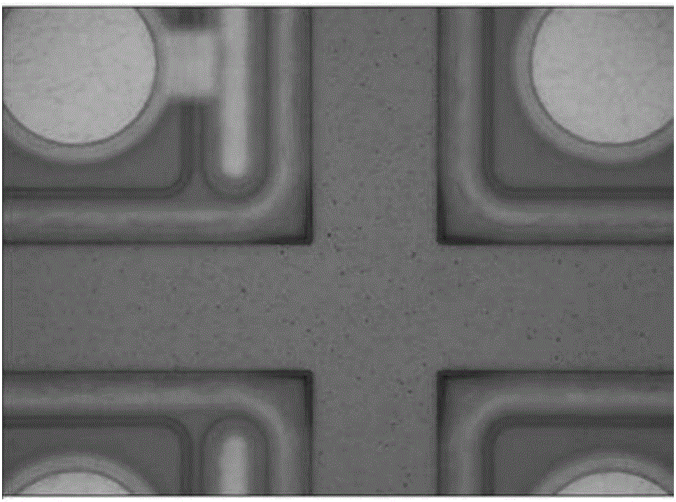
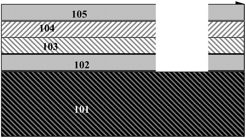
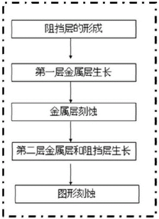
[0029] like figure 2 and Figure 3A As shown, a new method of metal wire film forming process of the present invention, the steps include:

[0030] 1) Form a first barrier layer 102 on the substrate 101 to prevent damage to the substrate 101 during metal film formation; the first barrier layer 102 has a film thickness of It is TiN or a composite material of Ti and TiN.

[0031] 2) Form the first metal layer 103 on the first barrier layer 102; this step mainly adopts the physical sputtering film forming process, and the film thickness of the first metal layer 103 is The sputtering temperature is 10-500°C, and the pressure is 1-10torr;

[0032] 3) A part of the first metal layer 103 is etched away by etching or other methods, and the film thickness ratio of the first metal layer 103 before and after etching is 100:90-1000:999; the etched ...


PUM


Abstract

The invention discloses a film forming process for a metal line, which mainly comprises the following steps: 1) forming a first barrier layer on a substrate; 2) forming a first metal layer on the first barrier layer; 3) etching one part of the first metal layer; 4) successively forming a second metal layer and a second barrier layer; and 5) performing pattern etching for forming the metal line. Through a manner of changing oriented growth of a metal aluminum film, the film forming process for the metal line has functions of: reducing etching residue of metal aluminum, preventing formation of metal black points in an etching trough, effectively improving device shortcircuit caused by the black points, and improving packaging quality of the device.

Description

technical field [0001] The invention belongs to the manufacturing process of semiconductor integrated circuits, and relates to a semiconductor film forming process, in particular to a metal wire film forming process method. Background technique [0002] The metal line film formation process has a crucial impact on the characteristics of semiconductor devices, especially the conduction resistance of the device. Due to the trend of semiconductor process integration, the performance of semiconductor chips is becoming more and more abundant, which is accompanied by the concentration of circuits caused by the degree of integration of semiconductor chips, and the increase in device heat generation, which ultimately affects the performance and service life of devices. [0003] like Figure 3B As shown, the traditional metal wire film-forming process generally adopts the following steps: first, a barrier layer is formed on the substrate, the first metal layer is grown on the barrier...

Claims


Application Information

Patent Timeline
Patent Type & Authority Patents(China)
IPC IPC(8): H01L21/768
CPCH01L21/76838H01L21/76841
Inventor 刘善善费强李晓远
Owner SHANGHAI HUAHONG GRACE SEMICON MFG CORP
Why Eureka
Try Eureka