
PCB preparation method and PCB
A technology for area and connecting lines, applied in chemical/electrolytic methods to remove conductive materials, printed circuit manufacturing, printed circuits, etc., can solve problems affecting the efficiency of PCB processing and preparation of wiring density, reduce the number of layouts, and increase wiring density Effect
- Summary
- Abstract
- Description
- Claims
- Application Information
AI Technical Summary
Problems solved by technology
Method used
Image

Examples
Embodiment Construction
[0034] Embodiments of the present invention are described in detail below, and examples of the embodiments are shown in the drawings, wherein the same or similar reference numerals denote the same or similar elements or elements having the same or similar functions throughout. The embodiments described below by referring to the figures are exemplary and are intended to explain the present invention and should not be construed as limiting the present invention.
[0035] The technical solutions of the present invention will be further described below in conjunction with the accompanying drawings and through specific implementation methods.
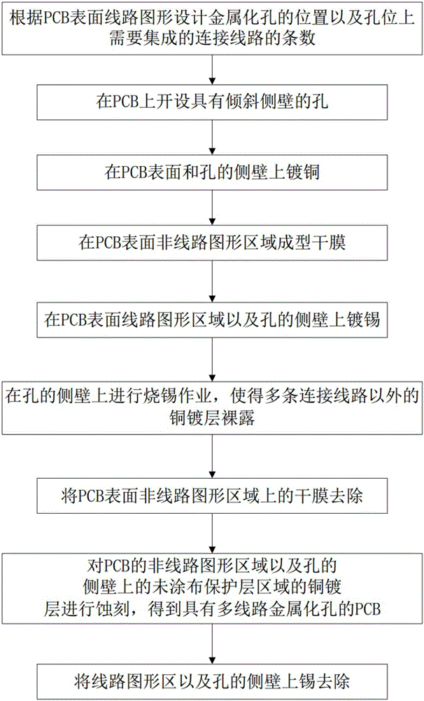
[0036] Such as figure 1 Shown, the present invention provides a kind of PCB preparation method, and it comprises the steps:
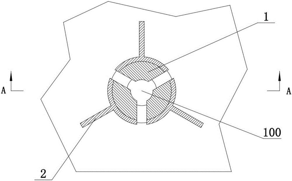
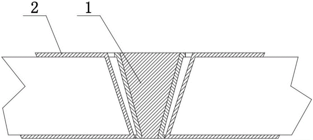
[0037] Step 1: Design the position of the metallized hole and the number of connecting lines 1 to be integrated on the hole position according to the circuit pattern 2 on the surface of the PCB.
[0038] In this ste...
PUM
 Abstract
Description
Claims
Application Information