Semiconductor device mounting board, method of manufacturing the same, method of inspecting the same, and semiconductor package

A semiconductor and mounting board technology, applied in the direction of semiconductor devices, semiconductor/solid-state device components, electric solid-state devices, etc., can solve problems such as difficulty in manufacturing external terminals, inability to obtain packaging reliability, defects, etc.

Inactive Publication Date: 2005-08-17
NEC CORP
View PDF5 Cites 17 Cited by
  • Summary
  • Abstract
  • Description
  • Claims
  • Application Information

AI Technical Summary

Problems solved by technology

However, since the external terminals are formed by etching, there is a problem that it is difficult to manufacture external terminals with a narrow pitch due to the limited control of the number of side etchings in the etching step
In addition, when the package wiring board is mounted on an external board or device, since stress concentrates on the boundary between the external terminal and the insulator film, causing a noticeable defect, sufficient package reliability cannot be obtained

Method used


Image

  • Semiconductor device mounting board, method of manufacturing the same, method of inspecting the same, and semiconductor package
  • Semiconductor device mounting board, method of manufacturing the same, method of inspecting the same, and semiconductor package
  • Semiconductor device mounting board, method of manufacturing the same, method of inspecting the same, and semiconductor package

Examples


Embodiment Construction

[0174] Next, referring to the drawings, an embodiment of the present invention will be described in detail. First, embodiments of a semiconductor device mounting board and a semiconductor package according to the present invention will be described. Hereinafter, the semiconductor device mounting board is referred to as "mounting board".

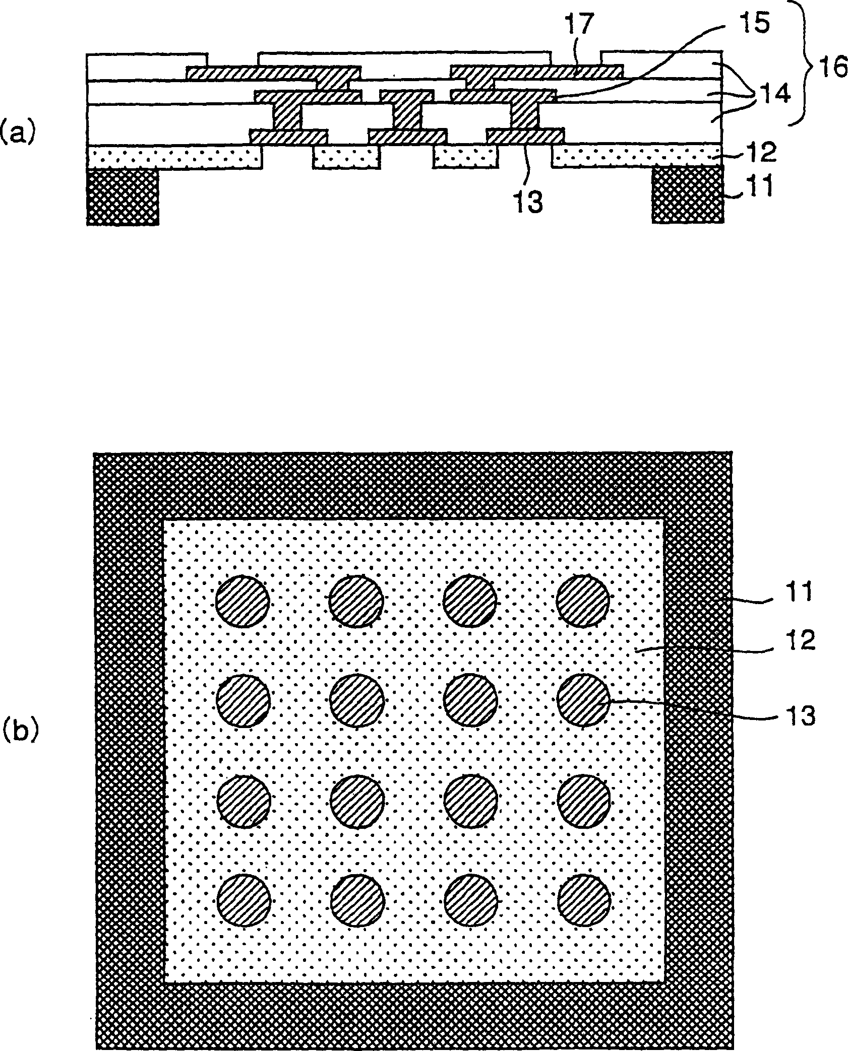
[0175] A first embodiment of a semiconductor device mounting board and a semiconductor package will be described. figure 1 A diagram showing the configuration of a semiconductor device mounting board according to the present invention, in which figure 1 (a) is the profile of the section view, figure 1 (b) is the rear profile seen from the side of the metal carrier 11 .

[0176] figure 1 The mounting board shown in (a) and (b) includes: a first electrode pattern 13 positioned on one surface of a wiring structure film 16 including an insulating layer 14 and a wiring layer; a second electrode pattern 17 on the opposite surface of the wiring...


PUM


Abstract

A semiconductor device mounting board in which high density packaging and fining can be realized in response to smaller pitches while ensuring excellent reliability of package by improving a conventional wiring board, its producing method and inspecting method, and a semiconductor package. The semiconductor device mounting board in characterized by comprising a wiring structure film consisting of an insulation layer and a wiring layer, a first electrode pattern provided on one surface of the wiring structure film such that at least the side circumference thereof touches the insulation layer but at least the lower surface thereof does not touch the insulation layer and the surface of the insulation layer provided with the first electrode pattern is coplanar with the lower surface of the first electrode pattern, a second electrode pattern formed on the surface opposite to the first electrode pattern, an insulator film provided with an opening pattern being confined in the first electrode pattern, and a metal support provided on the surface of the insulator film.

Description

technical field [0001] The present invention relates to a semiconductor device mounting board for realizing a module with high density, high speed and high frequency by mounting various devices such as semiconductor devices at high density, its manufacturing method, its inspection method, and semiconductor packaging and / or high frequency systems. Background technique [0002] Recently, as the speed and integration of semiconductor devices increase, the number of terminals increases and the pitch decreases, package wiring boards are also desired to have higher density and finer pitch to mount these semiconductor devices thereon. Currently widely used mounting boards are, for example, ceramic substrates, buildup substrates and tape substrates. [0003] As disclosed in Japanese Patent Laid-Open Publication No. 8-330474, a ceramic substrate includes an insulator substrate made of alumina and the like and a wiring conductor formed on the surface thereof made of, for example, W o...

Claims


Application Information

Patent Timeline
Patent Type & Authority Applications(China)
IPC IPC(8): H01L23/12H01L23/13H01L23/14H01L23/16H01L23/31H01L23/498
CPCH01L2924/01046H01L23/3121H01L2221/68345H01L2924/01079H01L2224/73204H01L2224/16H01L2224/73253H01L2924/01019H01L23/49822H01L2924/01078H01L2924/01057H01L23/13H01L23/16H01L2924/19041H01L2224/05568H01L2224/05573H01L2224/16235
Inventor 菊池克下户真典马场和宏
Owner NEC CORP
Why Eureka
Try Eureka