Manufacturing method for multi-layer high-density interconnected printed circuit board

A high-density interconnection and printed circuit board technology, which is applied in the direction of multilayer circuit manufacturing, printed circuit components, electrical connection printed components, etc., can solve the complex process of multilayer printed circuit boards, the line accuracy cannot be guaranteed, the process Complexity and other issues, to achieve the effect of reducing the production cycle, reducing the size of the board surface, and simplifying the process

Active Publication Date: 2008-11-26
JIANGNAN INST OF COMPUTING TECH
View PDF0 Cites 16 Cited by
  • Summary
  • Abstract
  • Description
  • Claims
  • Application Information

AI Technical Summary

Problems solved by technology

[0006] However, the above-mentioned process of manufacturing a multilayer printed circuit board is too complicated, and it needs to go through the process of making a wiring layer→laying a conductive layer→applying a dry film→making a copper pillar pattern→electroplating→……
The process of this process is relatively complicated. In steps 6 and 7, after removing the dry film and etching the conductive layer, the conductive layer needs to be deposited again, and the production cycle is too long; moreover, due to the need to etch twice before and after, the accuracy of the line Not guaranteed, critical for HDI PCBs with characteristic impedance requirements

Method used


Image

  • Manufacturing method for multi-layer high-density interconnected printed circuit board
  • Manufacturing method for multi-layer high-density interconnected printed circuit board
  • Manufacturing method for multi-layer high-density interconnected printed circuit board

Examples


Embodiment 1

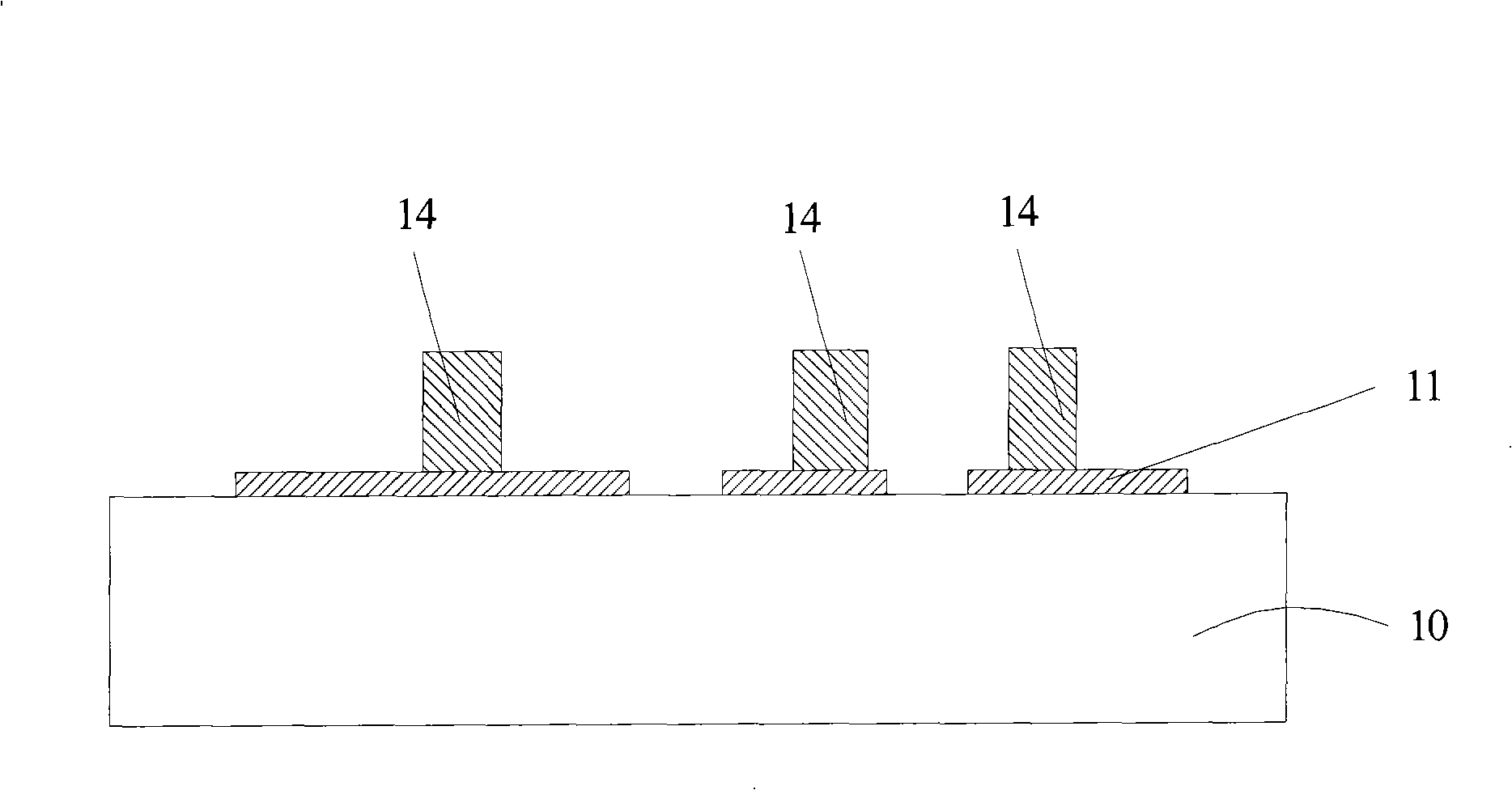
[0027] This embodiment provides a method for manufacturing a multilayer high-density interconnection printed circuit board. Refer to the attached Figure 4 In the process flow diagram shown, in step S300, a substrate is provided, and one or two circuit planes of the substrate have a first wiring layer, and the first wiring layer is formed on the first wiring layer for interconnection between the wiring layers. a first conductive bump,

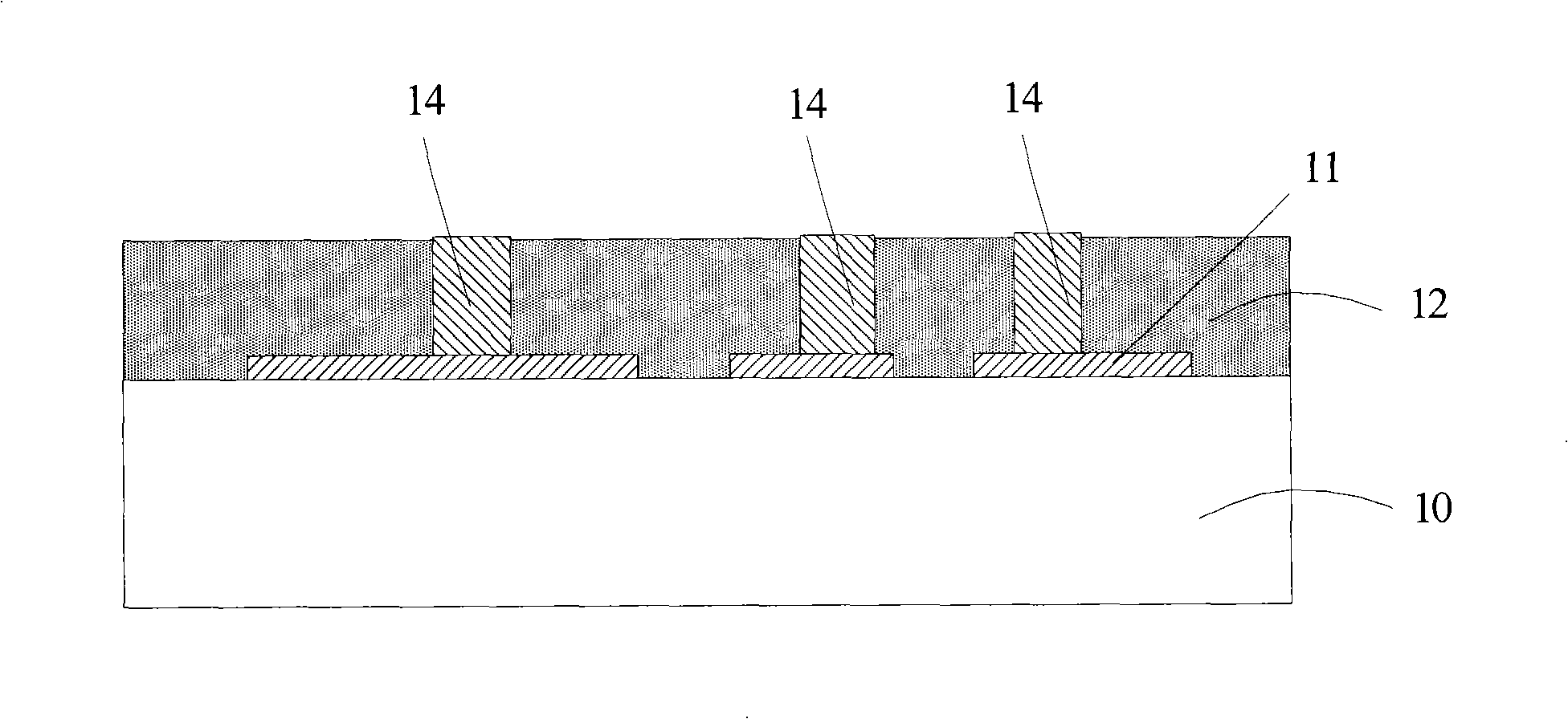
[0028] Step S301, 1) forming an insulating medium layer covering the first wiring layer and the first conductive bump on the substrate, and performing planarization treatment to expose the end surface of the first conductive bump;

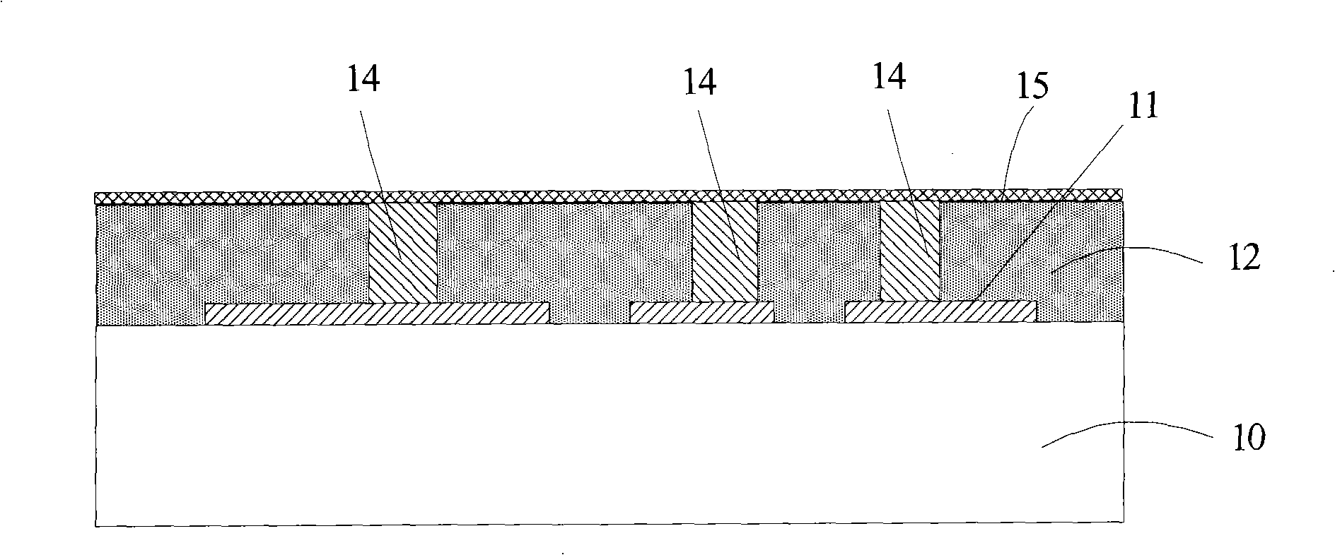
[0029] Step S302, 2) forming a conductive layer on the insulating dielectric layer;

[0030] Step S303, 3) forming a first insulating layer on the conductive layer and forming a second wiring layer pattern on the first insulating layer;

[0031] Step S304, 4) depositing a conductive material on the conductive laye...


PUM


Abstract

The invention relates to a production method of multilayer high-density interconnection printed circuit board, wherein one or two circuit faces of the baseboard are provided with a first wiring layer, the first wiring layer is formed with a first conductive block for interconnecting the wiring layers. The production method comprises: forming an insulated medium layer covering the first wiring layer and a first conductive block on the baseboard, forming a conductive layer on the insulated medium layer, forming a first insulated layer on the conductive layer and forming a second wiring layer picture on the first insulated layer, depositing conductive material to form a second wiring layer, forming a second insulated layer on the second wiring layer and the first insulated layer, etching the second insulated layer to form an opening exposing the second wiring layer, depositing the second conductive block in the opening, deleting the second insulated layer, the first insulated layer and the conductive layer under the first insulated layer, repeating aforementioned processes to form a multilayer high-density interconnection printed circuit board. The method simplifies the production.

Description

technical field [0001] The invention relates to the technical field of printed circuit board manufacturing, in particular to a method for manufacturing a multilayer high-density interconnected printed circuit board. Background technique [0002] In recent years, the design of various electronic products has become increasingly light, thin, short, and small, resulting in the relative miniaturization and weight reduction of various electronic components or printed circuit boards used to install electronic components. Therefore, the high density of printed circuit boards requirements are also increasing. In order to achieve a high-density printed circuit board, the method of increasing the wiring density in the wiring layer can be used, and the method of stacking the wiring layers into multiple layers to form a multilayer printed circuit board can also be used. [0003] A conventional method of manufacturing a multilayer high-density interconnection printed circuit board is a ...

Claims


Application Information

Patent Timeline
Patent Type & Authority Applications(China)
IPC IPC(8): H05K3/46H05K1/11H05K1/09
Inventor 吴小龙吴梅珠徐杰栋刘秋华郭双全张伯兴
Owner JIANGNAN INST OF COMPUTING TECH
Why Eureka
Try Eureka