Method for wafer-level manufacturing of objects and corresponding semi-finished products

a manufacturing method and technology for objects, applied in applications, other domestic articles, transportation and packaging, etc., can solve the problems of increased reproducibility, increased processing time and cost, etc., and achieve the effects of improving process stability in manufacturing, improving manufacturability of wafer-level manufacturing, and improving handling

Active Publication Date: 2014-10-02
AMS SENSORS SINGAPORE PTE LTD
View PDF5 Cites 15 Cited by
  • Summary
  • Abstract
  • Description
  • Claims
  • Application Information

AI Technical Summary

Benefits of technology

[0016]Another object of the invention is to provide a way of manufacturing objects which provides an improved handling during the manufacturing, in particular in wafer-level manufacturing.
[0017]Another object of the invention is to provide an improved process stability in the manufacture of objects, in particular in wafer-level manufacturing.
[0018]Another object of the invention is to provide an improved manufacturability in wafer-level manufacturin

Problems solved by technology

Wafer-level processing usually saves processing time an

Method used


Image

  • Method for wafer-level manufacturing of objects and corresponding semi-finished products
  • Method for wafer-level manufacturing of objects and corresponding semi-finished products
  • Method for wafer-level manufacturing of objects and corresponding semi-finished products

Examples


Embodiment Construction

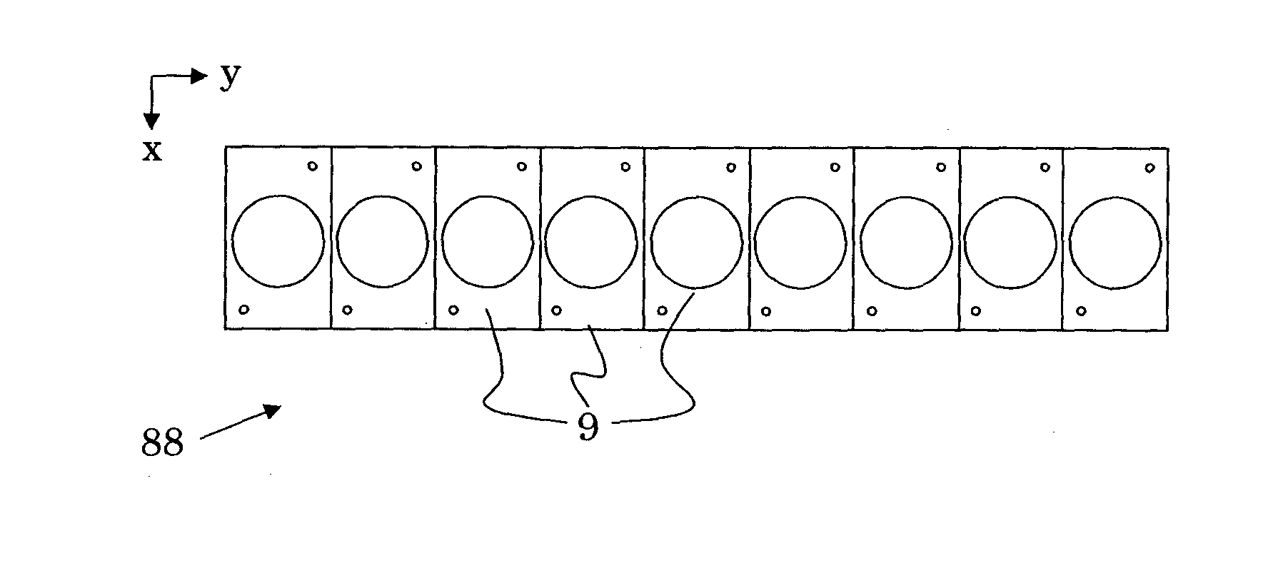
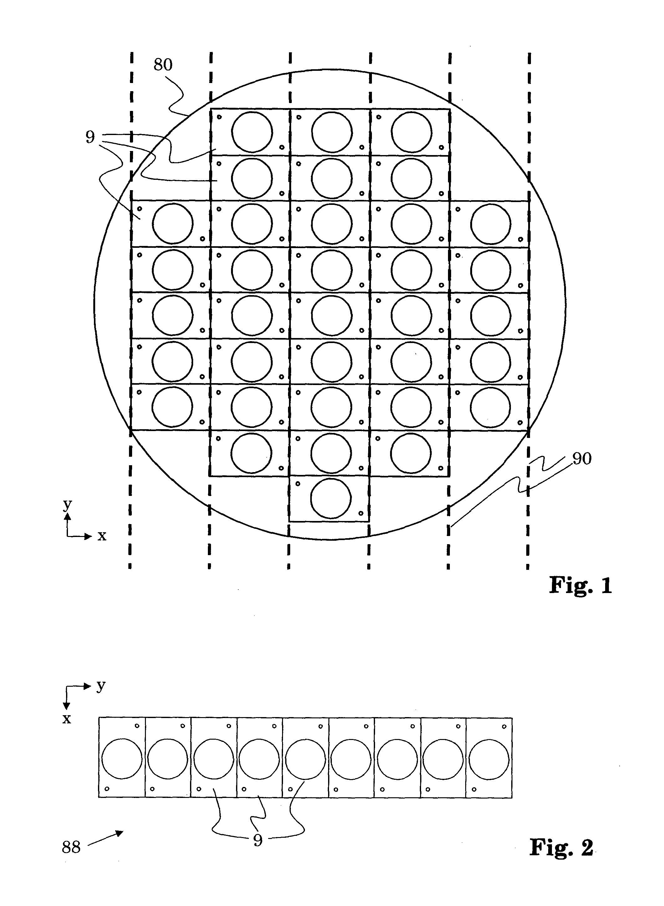
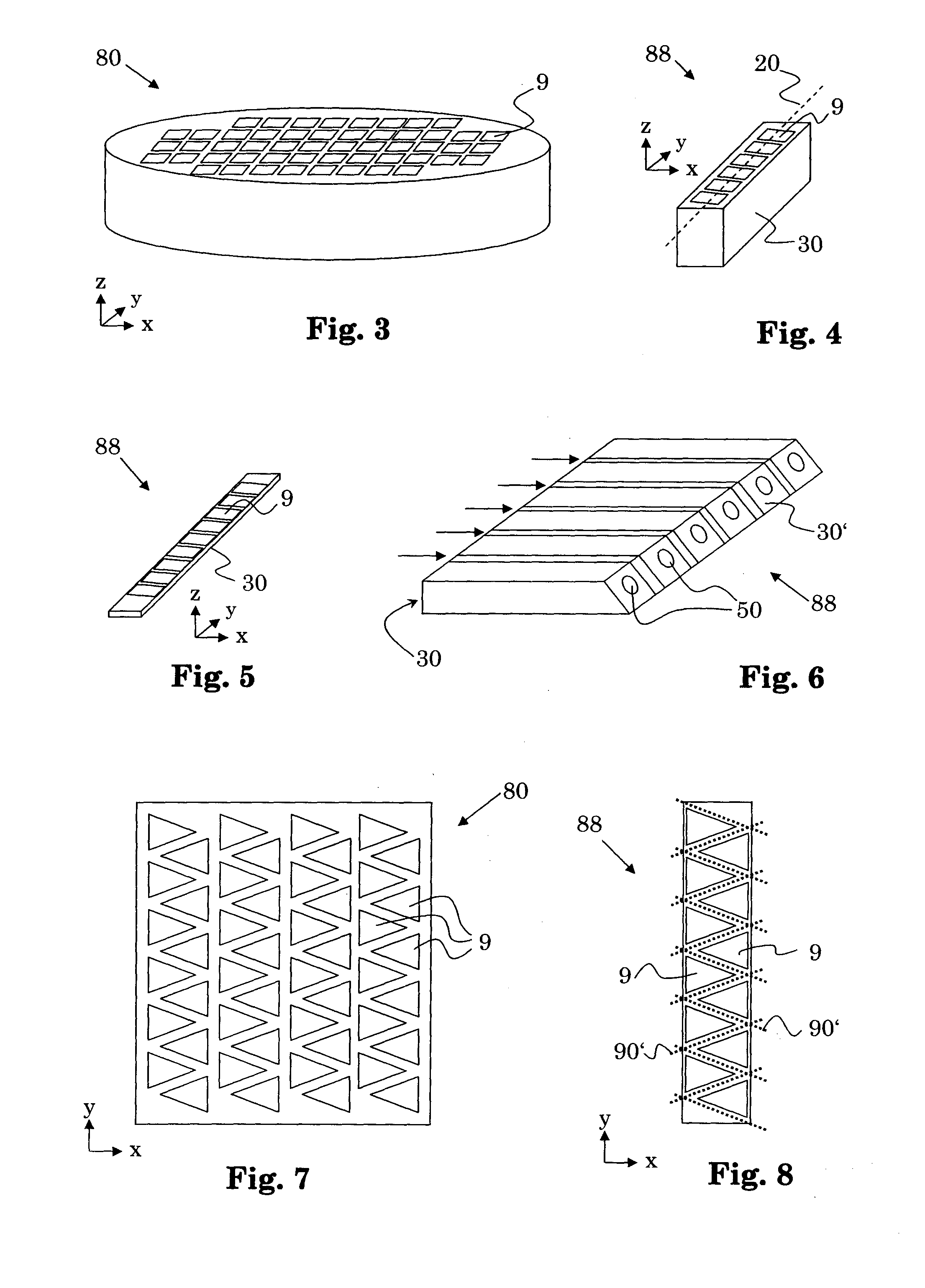
[0127]FIG. 1 is a schematic illustration of a wafer 80 comprising a multitude of semi-finished objects 9, in a top view. FIG. 1 shows a lateral plane. Therein, the coordinates x and y are located, whereas the vertical direction (z) is perpendicular to the drawing plane.

[0128]Various processes may have been applied to wafer 80 in order to produce semi-finished objects 9. Semi-finished objects 9 may, e.g., be optical systems or other systems or elements or items, such as MEMS or microelectronic devices or opto-electronic modules or others mentioned elsewhere in the present patent application.

[0129]In conventional wafer-level processing, wafer 80 would be separated, e.g., by sawing, not only along separating lines (sometimes also referred to as “dicing streets”) 90, but also along lateral lines perpendicular thereto (not shown in FIG. 1). The result would be numerous separated semi-finished objects 9, i.e. semi-finished objects which are not connected to each other anymore. In fact the...


PUM

PropertyMeasurementUnit
Shapeaaaaaaaaaa
Transparencyaaaaaaaaaa
Refractionaaaaaaaaaa

Abstract

The method for manufacturing an object comprises the steps of (a) providing a wafer comprising a multitude of semi-finished objects; (b) separating said wafer into parts referred to as sub- wafers, at least one of said sub-wafers comprising a plurality of said semi-finished objects; (c) processing at least a portion of said plurality of semi-finished objects by subjecting said at least one sub-wafer to at least one processing step; and preferably also the step of (d) separating said at least one sub-wafer into a plurality of parts.

Description

RELATED APPLICATIONS[0001]Incorporated by reference is U.S. provisional application with Ser. No. 61 / 418017 filed on Nov. 30, 2010 and the PCT application published on Jun. 7, 2012 with publication number WO 2012 / 071674 A1 claiming priority of said U.S. provisional application 61 / 418017.TECHNICAL FIELD[0002]The invention relates to a novel method for manufacturing objects, in particular small objects, and to a corresponding semi-finished product. More particularly, it relates to wafer-level manufacturing of objects. The invention relates to methods and products according to the opening clauses of the claims. The invention may find application, e.g., in the fields of micro-optics, micro-mechanics, micro-electromechanics and microelectronics.BACKGROUND OF THE INVENTION[0003]Wafer-level processing of objects such as optical systems and micro-electromechanical systems (MEMS) and microelectronic devices are well known in the art. Various types of processes such as replication processes, ...

Claims


Application Information

Patent Timeline
IPC IPC(8): B81B7/04B81C1/00
CPCH01L27/14618H01L27/14685B81C1/00904B81B7/04H01L27/14696H01L2924/0002Y10T428/18Y10T29/49002B29D11/00663B29D11/00307H01L2924/00
Inventor RIEL, PETERRUDMANN, HARTMUTROSSI, MARKUS
Owner AMS SENSORS SINGAPORE PTE LTD
Why Eureka
Try Eureka