A Method for Analyzing Wafer Defects of Various Products

An analysis method and defect analysis technology, which is applied in the field of analysis of wafer defects of various products, to achieve the effect of overcoming time-consuming and labor-intensive improvements in defect levels

Active Publication Date: 2019-12-17
CHINA RESOURCES MICROELECTRONICS (CHONGQING) CO LTD
View PDF6 Cites 0 Cited by
  • Summary
  • Abstract
  • Description
  • Claims
  • Application Information

AI Technical Summary

Problems solved by technology

[0002] Wafer defect analysis refers to the analysis of defects on the wafer, which is convenient for technicians to find problems and improve them according to the defects, and improve the process level. There are many types of existing wafer mass-produced products, and it is impossible to achieve the defect level of each product. All can be monitored, that is, it is necessary to analyze the defect level of multiple product combinations on the same platform, but there are great differences in the grain size and number of grains of each product. When performing defect scanning, products with more grains can be scanned effectively The area is smaller than that of products with fewer grains. If n particles are randomly scattered, due to the difference in scanning area, the number of defects detected on products with more grains is less than that of products with fewer grains (defects are randomly distributed). If With the current analysis method, it is impossible to accurately mix products with different grain numbers together to analyze the level of defects

Method used


Image

  • A Method for Analyzing Wafer Defects of Various Products
  • A Method for Analyzing Wafer Defects of Various Products
  • A Method for Analyzing Wafer Defects of Various Products

Examples


Embodiment Construction

[0029] The following will clearly and completely describe the technical solutions in the embodiments of the present invention with reference to the accompanying drawings in the embodiments of the present invention. Obviously, the described embodiments are only some, not all, embodiments of the present invention. Based on the embodiments of the present invention, all other embodiments obtained by persons of ordinary skill in the art without creative efforts fall within the protection scope of the present invention.

[0030] It should be noted that, in the case of no conflict, the embodiments of the present invention and the features in the embodiments can be combined with each other.

[0031] The present invention will be further described below in conjunction with the accompanying drawings and specific embodiments, but not as a limitation of the present invention.

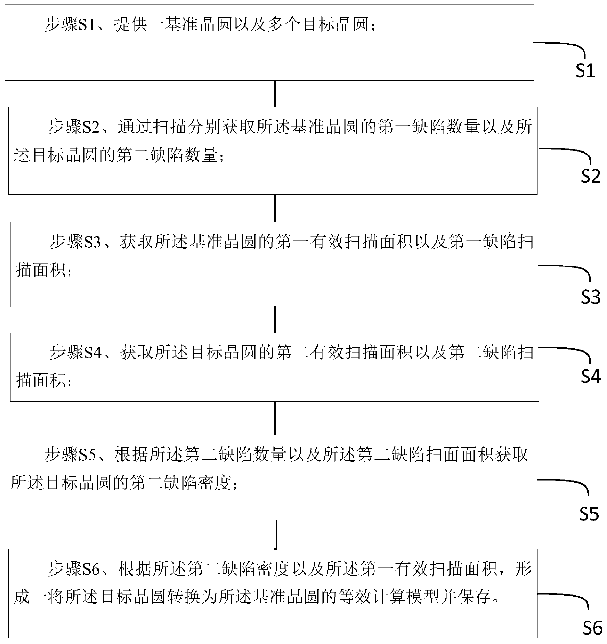
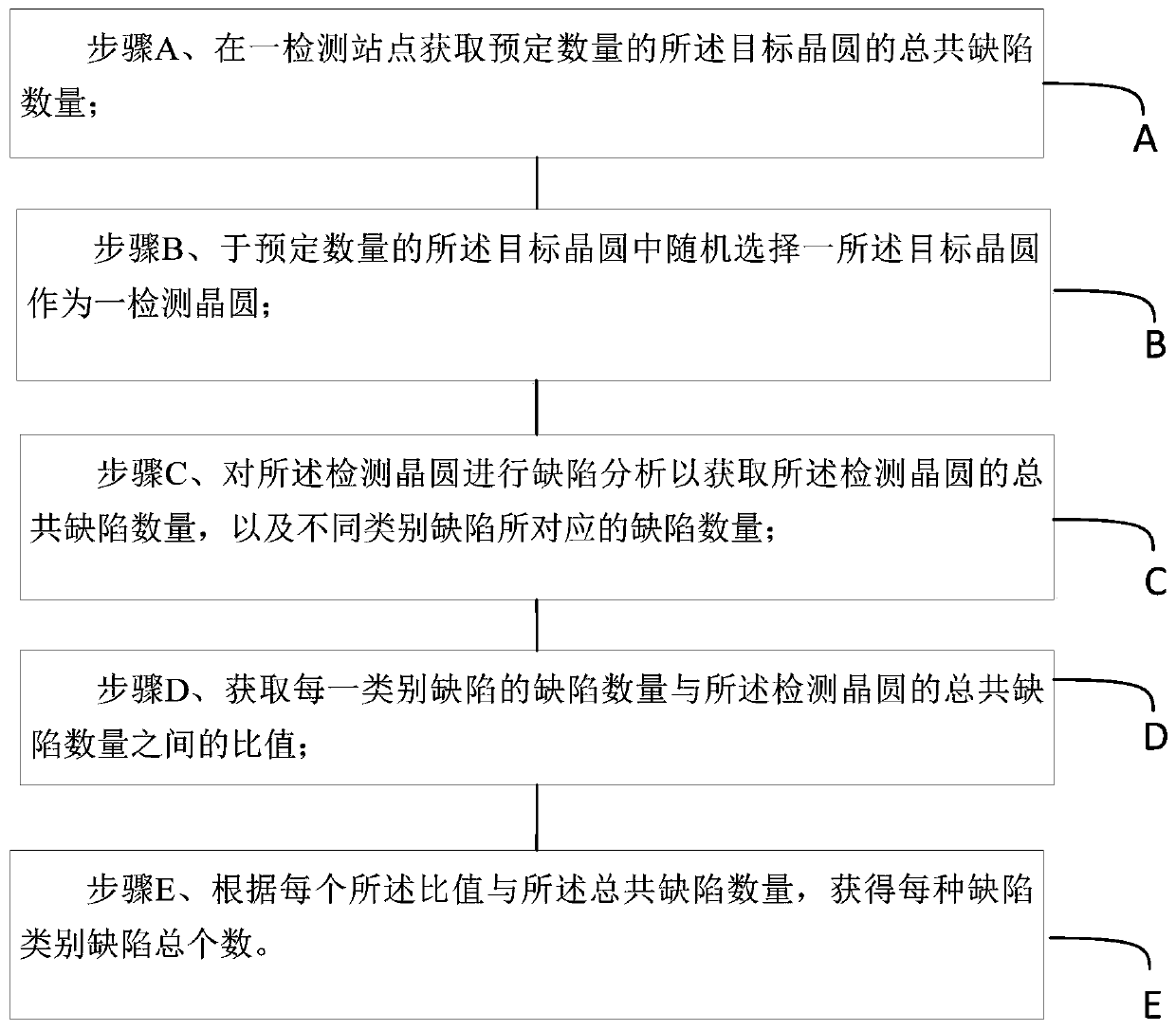
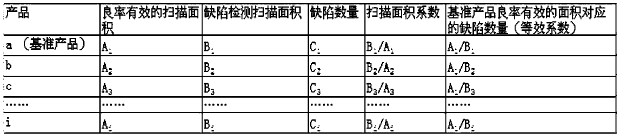
[0032] The technical solution of the invention includes a method for analyzing defects of various product wafers...


PUM


Abstract

The invention provides an analysis method for wafer defects of various products. The analysis method is applied to wafer defect analysis and characterized by particularly including the steps: providing a reference wafer and a plurality of target wafers; acquiring the number of first defects of the reference wafer and the number of second defects of the target wafers by scanning; acquiring the first effective scanning area of the reference wafer and the scanning area of the first defects; acquiring the second effective scanning area of the target wafers and the scanning area of the second defects; acquiring the second defect density and the first effective scanning area of the target wafers according to the number of the second defects and the scanning area of the second defects to form anequivalent calculation model for transforming the target wafers into reference wafers, and storing the equivalent calculation model. The analysis method has the advantages that the level of a certaindefect category on a production line (various products) can be objectively and accurately analyzed, and corresponding equipment of an engineering department is assisted in improvement of the defect level.

Description

technical field [0001] The invention relates to the technical field of semiconductor manufacturing, in particular to an analysis method for wafer defects of various products. Background technique [0002] Wafer defect analysis refers to the analysis of defects on the wafer, which is convenient for technicians to find problems and improve them according to the defects, and improve the process level. There are many types of existing wafer mass-produced products, and it is impossible to achieve the defect level of each product. All can be monitored, that is, it is necessary to analyze the defect level of multiple product combinations on the same platform, but there are great differences in the grain size and number of grains of each product. When performing defect scanning, products with more grains can be scanned effectively The area is smaller than that of products with fewer grains. If n particles are randomly scattered, due to the difference in scanning area, the number of ...

Claims


Application Information

Patent Timeline
Patent Type & Authority Patents(China)
IPC IPC(8): H01L21/66
CPCH01L22/12H01L22/20
Inventor 杜丽杨林曹兴旺
Owner CHINA RESOURCES MICROELECTRONICS (CHONGQING) CO LTD
Why Eureka
Try Eureka