Test device for chip detection

A chip detection and testing device technology, applied in measuring devices, electronic circuit testing, measuring electricity and other directions, can solve problems such as affecting the production speed of chips, and achieve the effect of facilitating the adjustment of the detection device, realizing timing rotation, and automatic detection and adjustment of the detection device.

Active Publication Date: 2019-02-22
中关村芯园(北京)有限公司
View PDF7 Cites 2 Cited by
  • Summary
  • Abstract
  • Description
  • Claims
  • Application Information

AI Technical Summary

Problems solved by technology

[0004] The invention provides a test device for chip detection, which has the advantages of automatic detection and easy adjustment of the detection device, and solves the problem that operators perform chip placement tests one by one and affect the production speed of chips

Method used


Image

  • Test device for chip detection
  • Test device for chip detection
  • Test device for chip detection

Examples


Embodiment Construction

[0023] The following will clearly and completely describe the technical solutions in the embodiments of the present invention with reference to the accompanying drawings in the embodiments of the present invention. Obviously, the described embodiments are only some, not all, embodiments of the present invention. Based on the embodiments of the present invention, all other embodiments obtained by persons of ordinary skill in the art without making creative efforts belong to the protection scope of the present invention.

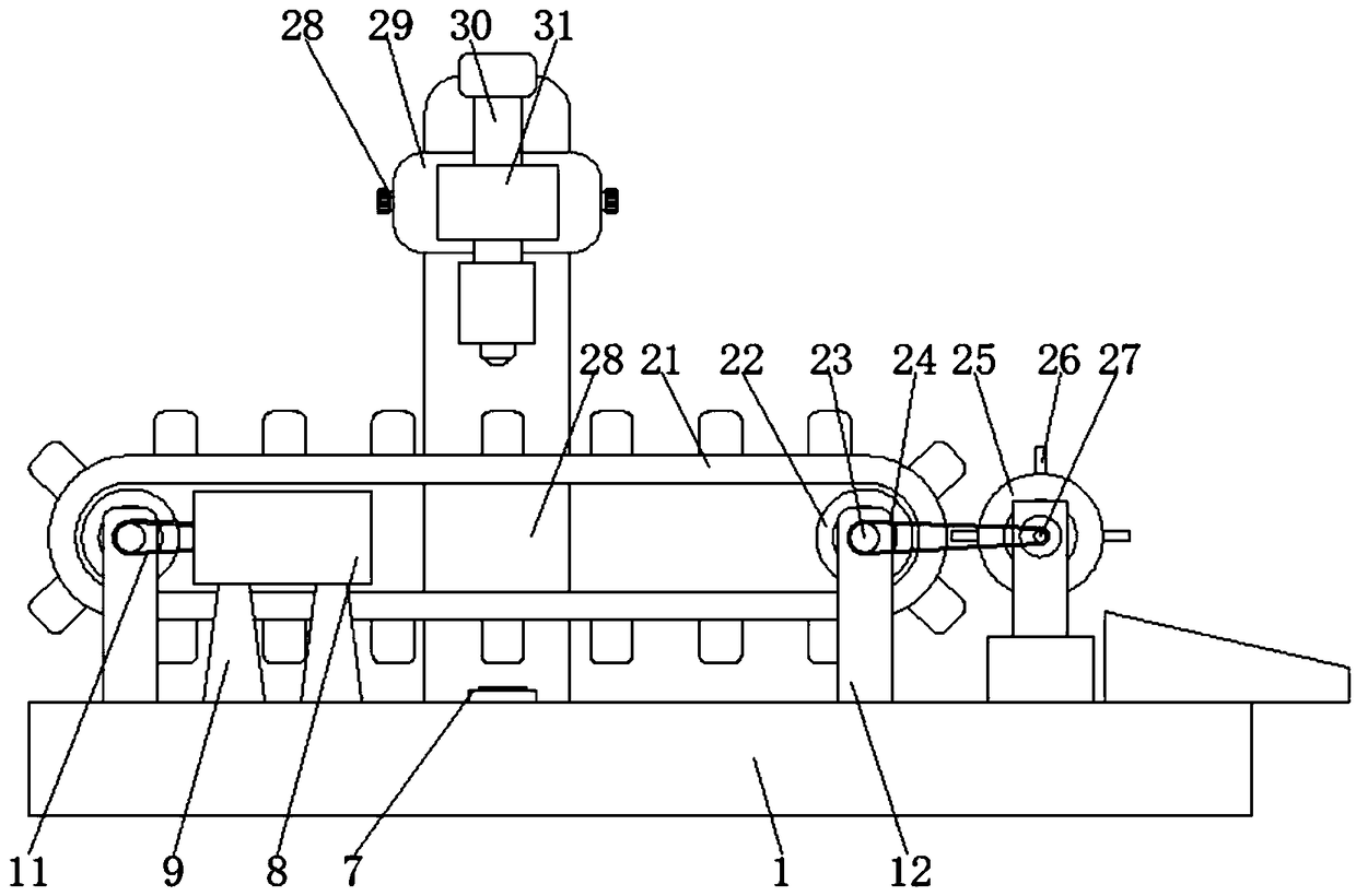
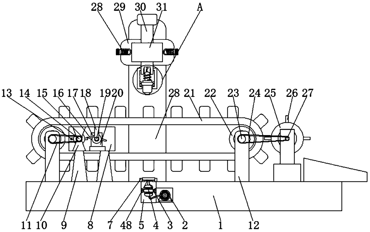
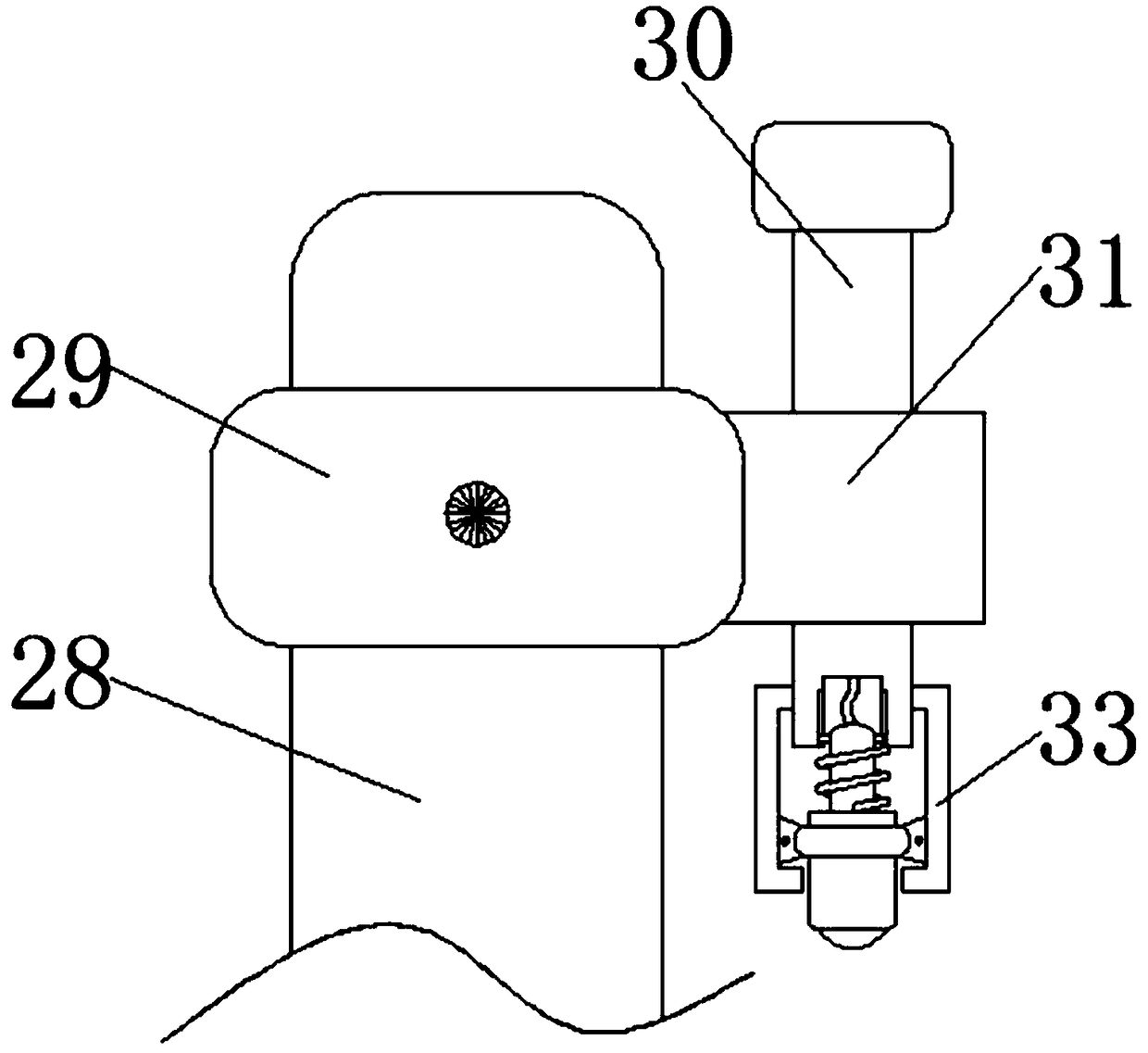
[0024] see Figure 1-5, a test device for chip detection, comprising a chip detection platform 1, a fixed rod 28 is fixedly installed on the top of the chip detection platform 1, a support 12 is fixedly installed on the top of the chip detection platform 1, the number of the support 12 is two, two The brackets 12 are distributed symmetrically around the axis of the chip testing platform 1. The insides of the two brackets 12 are movably connected with rolling d...


PUM


Abstract

The invention, which relates to the technical field of chip detection, discloses a test device for chip detection. The test device comprise a chip detection bench. A fixed rod is fixedly installed atthe top of the chip detection bench; two brackets are fixedly installed at the top of the chip detection bench and are distributed symmetrically by using the center of the axis of the chip detection bench; and roller rotating drums are movably connected inside the two brackets. A chip is placed inside a chip placing box and is pushed between two connecting plates by a push plate arranged at the top of a hydraulic rod; and a turntable is driven to make rotation by cooperating with a motor arranged inside the transmission box. A rotating rod is fixedly connected to the outer side of the turntable and is in contact with a lap joint plate arranged at the outer side of the rotating plate, so that the lap joint plate rotates regularly and a conveying belt is driven to rotate by cooperating witha first transmission belt; and thus the conveying belt rotates regularly to avoid continuous rotation, so that the incomprehensive detection of the chip is avoided.

Description

technical field [0001] The invention relates to the technical field of chip detection, in particular to a testing device for chip detection. Background technique [0002] A chip generally refers to the carrier of an integrated circuit, and is also the result of the design, manufacture, packaging, and testing of an integrated circuit. It is usually an independent whole that can be used immediately. The words "chip" and "integrated circuit" are often confused. Use, for example, in our usual discussion topics, integrated circuit design and chip design have the same meaning, and chip industry, integrated circuit industry, and IC industry often have the same meaning. In fact, these two words are related and have differences. Integration Circuit entities often exist in the form of chips, because integrated circuits in the narrow sense emphasize the circuit itself, such as a phase-shift oscillator that is as simple as only five components connected together. When it is still presen...

Claims


Application Information

Patent Timeline
Patent Type & Authority Applications(China)
IPC IPC(8): G01R31/28G01R31/01
CPCG01R31/013G01R31/2851
Inventor 不公告发明人
Owner 中关村芯园(北京)有限公司
Why Eureka
Try Eureka