Array substrate, display panel and display device

A technology of array substrates and substrate substrates, which is applied in the direction of electrical components, electric solid devices, circuits, etc., and can solve problems such as short circuit between gate lines and data lines, climbing disconnection, and difficulty in climbing data lines.

Active Publication Date: 2019-11-29
BOE TECH GRP CO LTD +1
View PDF6 Cites 2 Cited by
  • Summary
  • Abstract
  • Description
  • Claims
  • Application Information

AI Technical Summary

Problems solved by technology

[0004] The present invention provides an array substrate, a display panel, and a display device. The array substrate can solve the problem of difficulty in climbing a data line in the overlapping area of ​​a gate line and a data line, and generate broken lines wh

Method used


Image

  • Array substrate, display panel and display device
  • Array substrate, display panel and display device
  • Array substrate, display panel and display device

Examples


Embodiment Construction

[0029] The following will clearly and completely describe the technical solutions in the embodiments of the present invention with reference to the accompanying drawings in the embodiments of the present invention. Obviously, the described embodiments are only some, not all, embodiments of the present invention. Based on the embodiments of the present invention, all other embodiments obtained by persons of ordinary skill in the art without making creative efforts belong to the protection scope of the present invention.

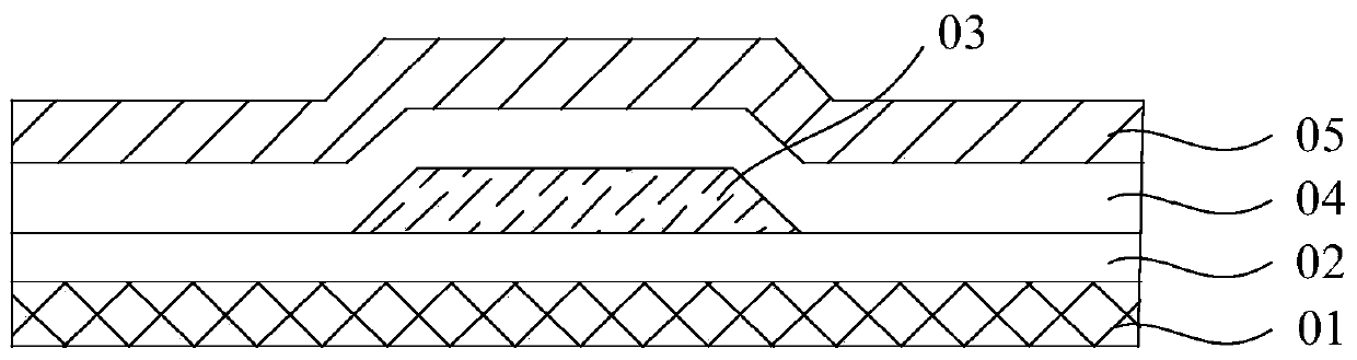
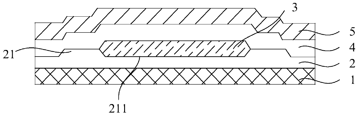
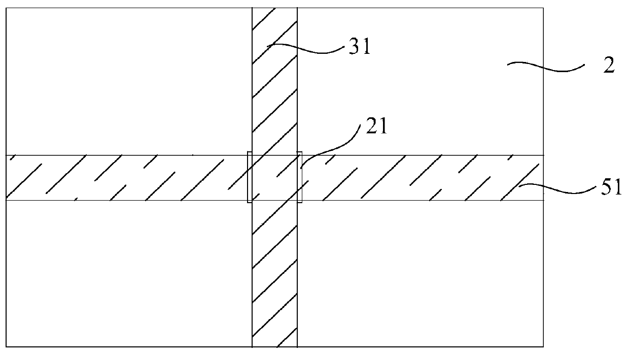
[0030] Please refer to figure 2 The present invention provides an array substrate, comprising a base substrate 1, a functional film layer 2 formed on one side of the base substrate 1, a gate line 3 formed on the side of the functional film layer 2 away from the base substrate 1, and a gate line 3 formed on the gate The interlayer insulating layer 4 on the side where the line 3 is away from the functional film layer 2, and the data line 5 formed on the side of...


PUM


Abstract

The invention relates to the technical field of display equipment, and discloses an array substrate, a display panel and a display device. The array substrate comprises an underlayer substrate, a functional film layer formed on one side of the underlayer substrate, a grid line formed on the side, which is away from the underlayer substrate, of the functional film layer, an interlayer insulating layer formed on the side, which is away from the functional film layer, of the grid line, and a data line formed on the side, which is away from the grid line, of the interlayer insulating layer, wherein the data line and the grid line are mutually crossed; fluctuation structures are formed on the two sides of the portion, which is opposite to the grid line, of the functional film layer, and the data line and the fluctuation structures are mutually crossed. According to the array substrate, the problems of difficult climbing and climbing line breakage of the data line in an overlapping region ofthe grid line and the data line are solved, the problem of short circuit between the grid line and the data line due to coverage of the interlayer insulating layer is solved, and adverse effects caused by lamination between the grid line and the data line are reduced.

Description

technical field [0001] The present invention relates to the technical field of display equipment, in particular to an array substrate, a display panel and a display device. Background technique [0002] For high-resolution display panel products, due to the increase in resolution, the line width of the conductive layer pattern decreases, and its thickness needs to be increased to meet the conductive requirements, such as figure 1 As shown, it is a schematic diagram of the intersection result of a conventional gate line and a data line, including: a base substrate 01 , a functional film layer 02 , a gate line 03 , an interlayer insulating layer 04 , and a data line 05 . [0003] Under the above circumstances, it will be difficult to climb the slope in the overlapping area of ​​the horizontal and vertical gate lines and data lines, and it is easy to cause a slope break, the diffusion of the gate metal film atoms will cause a short circuit, and the interlayer insulating layer 0...

Claims


Application Information

Patent Timeline
IPC IPC(8): H01L27/12
CPCH01L27/1244H01L27/1248
Inventor 胡迎宾赵策丁远奎宋威倪柳松刘军梁启斌罗标闫梁臣
Owner BOE TECH GRP CO LTD
Why Eureka
Try Eureka