Chip manufacture process and chip

A manufacturing process and chip technology, which is applied in the chip manufacturing process and the field of chips, can solve the problems of easy short circuit of chips and poor quality of finished products, and achieve the effects of high manufacturing reliability, stable connection, guaranteed quality of finished products and reliability of use

Inactive Publication Date: 2015-11-25
SEMICON MFG INT (SHANGHAI) CORP
View PDF4 Cites 4 Cited by
  • Summary
  • Abstract
  • Description
  • Claims
  • Application Information

AI Technical Summary

Problems solved by technology

[0006] This application aims to provide a chip manufacturing process and chip to solve the problems of easy short circuit and poor quality of finished products in the prior art

Method used


Image

  • Chip manufacture process and chip
  • Chip manufacture process and chip
  • Chip manufacture process and chip

Examples


Embodiment Construction

[0028] The embodiments of the application will be described in detail below with reference to the accompanying drawings, but the application can be implemented in many different ways defined and covered by the claims.

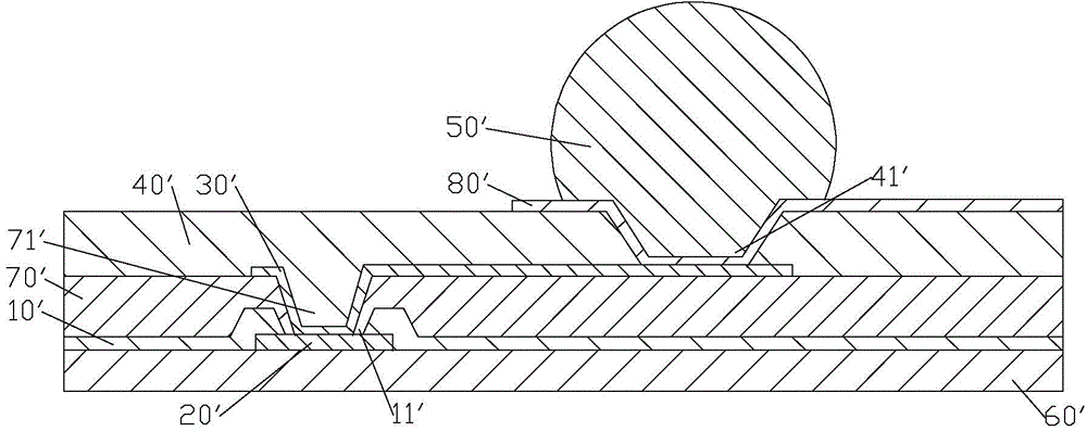
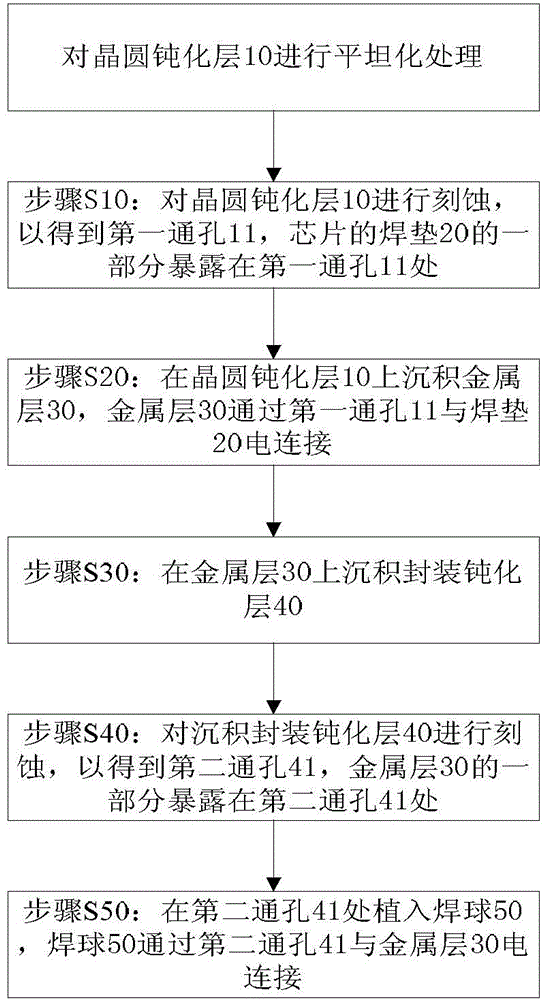
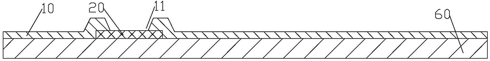
[0029] In order to solve the problems pointed out in the background art that chips are prone to short circuits and poor quality of finished products, the present application provides a chip manufacturing process. Such as Figure 2 to Figure 7 As shown, the chip manufacturing process includes planarizing the wafer passivation layer 10 . After the wafer passivation layer 10 is planarized, the surface of the wafer passivation layer 10 is flatter, the uneven feeling is reduced, and the fine grooves are eliminated, thus making the metal layer deposited on the wafer passivation layer 10 30 and the wafer passivation layer 10 are connected more firmly and evenly, thereby avoiding the loosening of the metal layer 30, and solving the problem that the metal layer 30 exte...


PUM


Abstract

The application provides a chip manufacture process and a chip. The chip manufacturing process comprises performing planarization treatment on a wafer passivation layer. After the wafer passivation layer is flattened, the surface is flatter, unevenness is reduced, and tiny grooves are eliminated, accordingly allowing more stable and uniform connection between the metal layer deposited on the wafer passivation layer and the wafer passivation layer, thereby avoiding the loosening of the metal layer, solving the problem of chip short circuit caused when the metal layer extends outwards along the groove of the wafer passivation layer to conduct with the peripheral metal layer, and furthermore guaranteeing chip finished product quality and serviceability; meanwhile the chip manufacture process of the application possesses the characteristics of simple preparation and high manufacture reliability.

Description

technical field [0001] The present application relates to the technical field of chip manufacturing, and more specifically, to a chip manufacturing process and a chip. Background technique [0002] Wafer-level packaging (WLP) is an advanced chip packaging technology. As semiconductor products have higher and higher market requirements for shortened development cycles, reduced costs, and reduced sizes, higher requirements are placed on the chip manufacturing process. Require. [0003] Such as figure 1 As shown, the common chip in the prior art is a standard four-layer packaging structure. A chip with a four-layer package structure includes a substrate 60', a bonding pad 20', a wafer passivation layer 10', an insulating layer 70', a metal layer 30', a package passivation layer 40', an under-ball metal layer 80' and The solder ball 50', wherein the solder pad 20' is disposed on the substrate 60', the wafer passivation layer 10' is disposed on the solder pad 20' and the subst...

Claims


Application Information

Patent Timeline
Patent Type & Authority Applications(China)
IPC IPC(8): H01L21/3105
Inventor 俞颖江博渊
Owner SEMICON MFG INT (SHANGHAI) CORP
Why Eureka
Try Eureka