Composite scab structure and producing method thereof

A technology of bumps and polymers, applied in semiconductor/solid-state device manufacturing, electrical components, electrical solid-state devices, etc., can solve problems such as deformation

Inactive Publication Date: 2005-02-23
AU OPTRONICS CORP
View PDF0 Cites 4 Cited by
  • Summary
  • Abstract
  • Description
  • Claims
  • Application Information

AI Technical Summary

Problems solved by technology

And because the elastic recovery force of the polymer of its compound bump structure is larger than that of the gold bump in the prior art, it can buffer the stress generated by the bonding between the semiconductor substrate and the glass substrate, and solve the problem of deformation

Method used


Image

  • Composite scab structure and producing method thereof
  • Composite scab structure and producing method thereof
  • Composite scab structure and producing method thereof

Examples


Embodiment Construction

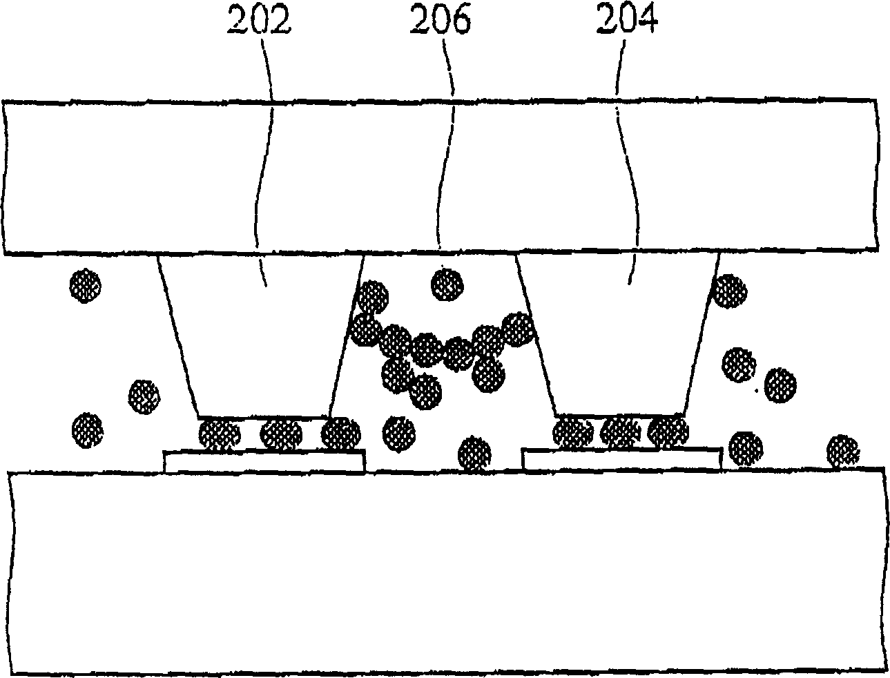
[0039] like Figure 4 As shown, the composite bump structure of this embodiment includes the following elements: a contact pad 402 is located on a substrate 400, such as a semiconductor substrate, electrodes (not shown) are formed on the substrate 400, and the contact pad 402 and The electrodes are electrically connected. The main part 404 is composed of a polymer, located on the substrate 400. The above-mentioned polymer is preferably a high molecular polymer, more preferably a high molecular polymer with a thermal expansion coefficient similar to that of metals such as aluminum and gold, and a good bond with the metal. .

[0040] The composite bump structure of this embodiment further includes at least one conductive plug 406 located in the main body portion 404 . In detail, the above-mentioned conductive plug 406 runs through the entire main body portion 404 ; and a conductive layer 408 is located on the main body portion 404 , wherein the conductive layer 408 is electric...


PUM


Abstract

The compound cam structure is composed of a base plate, a contacting pad located on the base plate, a main body comprised of the polymer on the contacting pad, a conducting socket in the main body, which interpenetrates the main body. The conducting layer connects with the conducting pad via the conducting socket and the protecting layer on the base plate covers part of the contacting pad.

Description

technical field [0001] The invention relates to a construction technology of an integrated circuit, in particular to a compound bump structure and a manufacturing method applied in the construction technology between an integrated circuit and a display. Background technique [0002] In some existing electronic devices, the connection between the components and the main circuit is performed through a conductive film (such as anisotropic conductive adhesive, or ACF for short). Anisotropic conductive adhesive ACF is made by mixing non-conductive synthetic resin and conductive particles. Conductive particles 1 such as Figure 1A As shown in the cross-sectional view of , its diameter is about 3-5 μm, its central part 1a is made of polymer, and the outside is covered with metal conductor 1b, such as gold, nickel, tin, etc. [0003] ACF is often used in the manufacture of liquid crystal displays, and some are used to directly package the driver chip of the panel on the glass substr...

Claims


Application Information

Patent Timeline
Patent Type & Authority Applications(China)
IPC IPC(8): H01L21/60H01L23/48
CPCH01L24/29H01L2224/16225H01L2224/73204H01L2224/32225H01L2224/83101H01L2924/14H01L2924/351
Inventor 陈慧昌李俊右
Owner AU OPTRONICS CORP
Why Eureka
Try Eureka