Array substrate and liquid crystal panel

An array substrate and substrate technology, which is applied in the field of liquid crystal display, can solve the problems of the influence of pixel aperture ratio and complicated control methods, and achieve the effect of improving color shift.

Active Publication Date: 2020-12-15
CHENGDU ZHONGDIAN PANDA DISPLAY TECH CO LTD
View PDF13 Cites 0 Cited by
  • Summary
  • Abstract
  • Description
  • Claims
  • Application Information

AI Technical Summary

Problems solved by technology

[0004] Eight-domain division is a commonly used division of pixel domains, but in ordinary eight-domain pixels, due to the use of a large number of thin film transistors and corresponding capacitors, the control method is more complicated, and the aperture ratio of the pixel will be affected. influences

Method used


Image

  • Array substrate and liquid crystal panel
  • Array substrate and liquid crystal panel
  • Array substrate and liquid crystal panel

Examples


Embodiment 1

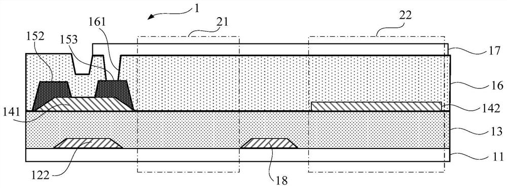
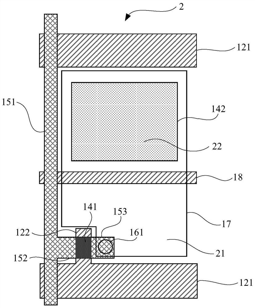
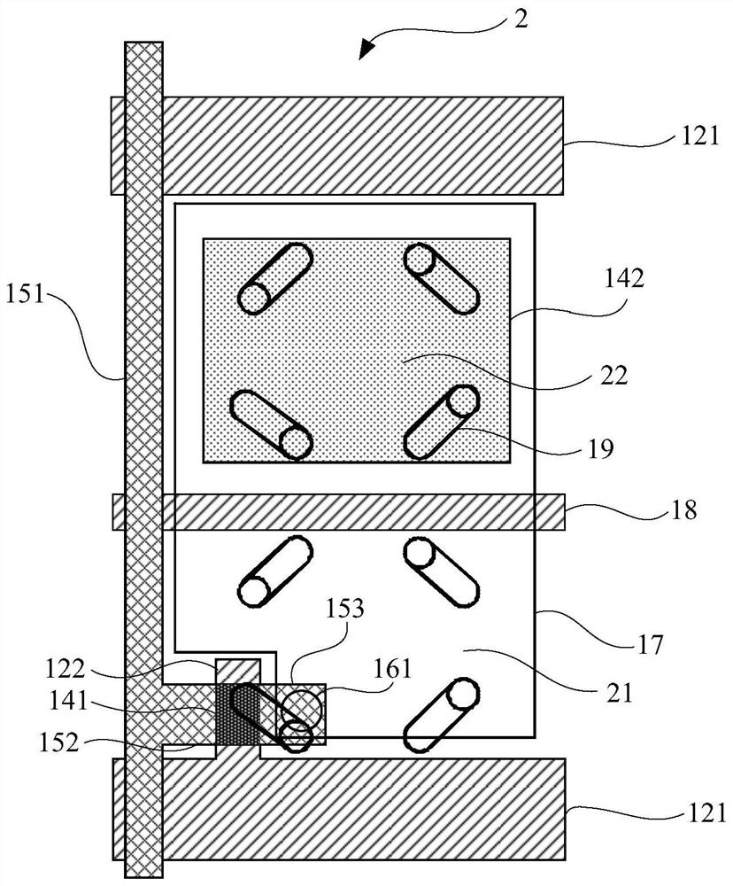
[0028] figure 1 A partial cross-sectional view of an array substrate provided in Embodiment 1 of the present invention; figure 2 for figure 1 top view of image 3 A schematic diagram of the eight-domain-like array substrate provided in Embodiment 1 of the present invention; Figure 4 A partial top view of another array substrate provided in Embodiment 1 of the present invention; Figure 5 A partial top view of the third array substrate provided in Embodiment 1 of the present invention; Figure 6 A partial top view of a fourth array substrate provided in Embodiment 1 of the present invention.

[0029] Such as Figure 1 to Figure 6 As shown, this embodiment provides an array substrate 1, the array substrate 1 includes a substrate 11, a gate 122 formed on the substrate 11, a gate insulating layer 13 covering the gate 122 and the substrate 11, and a gate insulating layer 13 formed on the gate insulating The active layer 141 on the layer 13 and the source electrode 152 and t...

Embodiment 2

[0068] This embodiment provides a liquid crystal panel. The liquid crystal panel may include a color filter substrate 11, a liquid crystal molecular layer, and the array substrate 1 described in Embodiment 1. The color filter substrate 11 and the array substrate 1 are arranged opposite to each other. between the substrate 11 and the array substrate 1 .

[0069] A liquid crystal panel usually consists of an array substrate 1, a color filter substrate 11, and a layer of liquid crystal molecules sandwiched between the array substrate 1 and the color filter substrate 11. By applying a driving voltage between the array substrate 1 and the color filter substrate 11, The rotation of the liquid crystal molecules 19 in the liquid crystal molecular layer can be controlled, so that the light emitted by the backlight source of the backlight module is refracted to generate a picture.

[0070] Wherein, the specific structure, function and working principle of the array substrate 1 have been...


PUM

PropertyMeasurementUnit
widthaaaaaaaaaa
widthaaaaaaaaaa

Abstract

The invention provides an array substrate and a liquid crystal panel. The array substrate provided by the invention comprises a substrate body, a grid electrode formed on the substrate body, a grid electrode insulating layer covering the grid electrode and the substrate body, an active layer formed on the grid electrode insulating layer, a source electrode and a drain electrode which are connectedwith the active layer, a plurality of sub-pixels which are separated into an array by criss-cross data lines and scanning lines, and a pixel electrode connected with the drain electrode through via holes. A shielding layer is further arranged on the grid electrode insulating layer, the shielding layer partially shields the pixel electrode, the shielding layer is of an island structure, and the light transmittance of the area covered by the shielding layer is lower than that of other light-transmitting areas. According to the array substrate, color cast can be improved, the structure is simple, and liquid crystal response is not affected.

Description

technical field [0001] The invention relates to the technical field of liquid crystal display, in particular to an array substrate and a liquid crystal panel. Background technique [0002] A liquid crystal panel is usually composed of a color filter substrate, an array substrate, and a liquid crystal molecular layer arranged between the two substrates. The opposite inner sides of the two substrates are respectively provided with a common electrode and a pixel electrode, and the liquid crystal molecules in the liquid crystal molecular layer are controlled by applying a voltage. Change the direction to refract the light from the backlight module to produce a picture. [0003] Currently, common display modes of liquid crystal panels mainly include TN (Twisted Nematic) mode, VA (Vertical Alignment Alignment) mode, IPS (In-Plane Switching) mode, and the like. Among them, the VA display mode refers to the mode in which the liquid crystal molecules are vertically aligned with the ...

Claims


Application Information

Patent Timeline
Patent Type & Authority Patents(China)
IPC IPC(8): G02F1/1362G02F1/1368G02F1/1335H01L27/12
CPCG02F1/133512G02F1/133514G02F1/136209G02F1/136286G02F1/1368H01L27/1237H01L27/1244
Inventor 李智炜薛彦鹏陈盈惠殷桂华胡珂罗艳梅刘翔储周硕李广圣孙学军
Owner CHENGDU ZHONGDIAN PANDA DISPLAY TECH CO LTD
Why Eureka
Try Eureka