Display panel, manufacturing method and electronic equipment

A technology for display panels and manufacturing methods, which is applied in the field of OLEDs and can solve problems such as damage to the packaging structure of glass cover plates and array substrates, affecting the packaging stability of small-sized OLED panels, etc.

Pending Publication Date: 2021-03-19
SHANGHAI TIANMA AM OLED
View PDF0 Cites 0 Cited by
  • Summary
  • Abstract
  • Description
  • Claims
  • Application Information

AI Technical Summary

Problems solved by technology

[0003] However, at present, after the glass cover plate and the array substrate are packaged, the current small-sized OLED panel cannot effectively discharge static electricity during the ESD (Electro-Static D

Method used


Image

  • Display panel, manufacturing method and electronic equipment
  • Display panel, manufacturing method and electronic equipment
  • Display panel, manufacturing method and electronic equipment

Examples


Embodiment Construction

[0036] The technical solutions in the embodiments of the present invention will be clearly and completely described below with reference to the accompanying drawings in the embodiments of the present invention. Obviously, the described embodiments are only a part of the embodiments of the present invention, but not all of the embodiments. Based on the embodiments of the present invention, all other embodiments obtained by those of ordinary skill in the art without creative efforts shall fall within the protection scope of the present invention.

[0037] In order to make the above objects, features and advantages of the present invention more clearly understood, the present invention will be described in further detail below with reference to the accompanying drawings and specific embodiments.

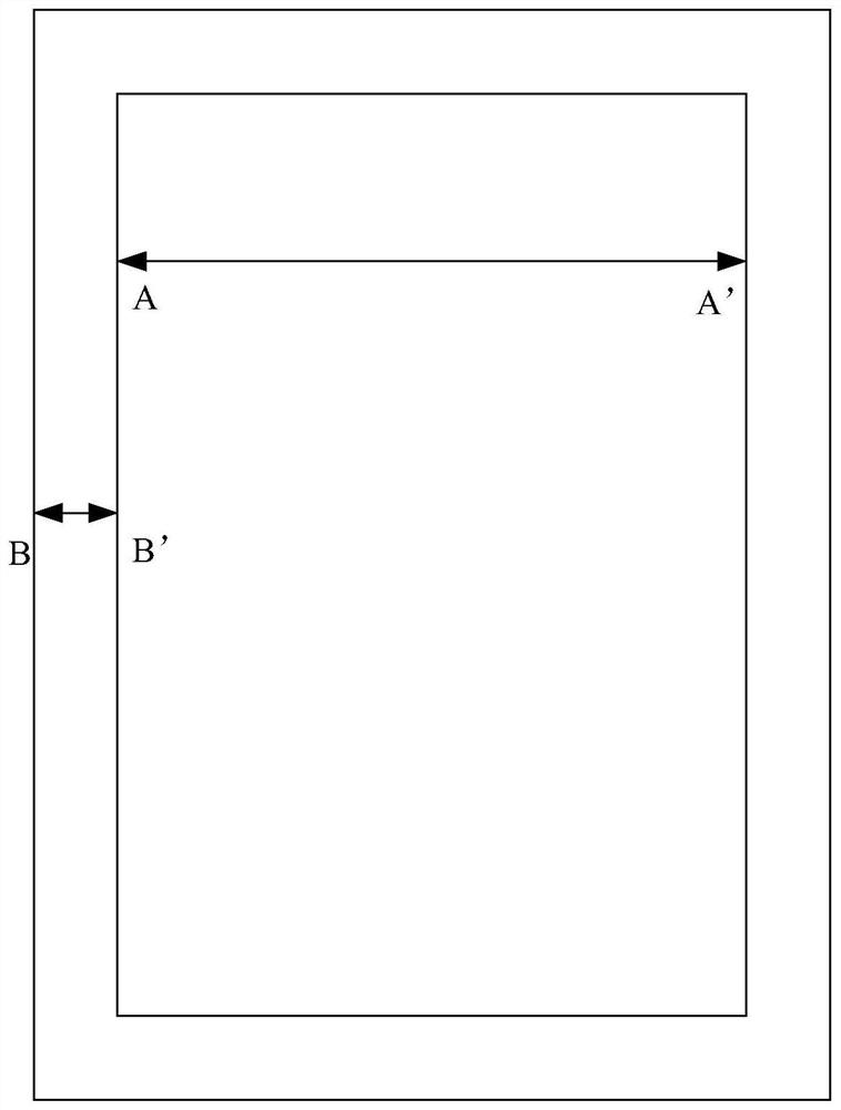
[0038] refer to figure 1 , figure 1 This is a schematic top view of a display panel according to an embodiment of the present invention.

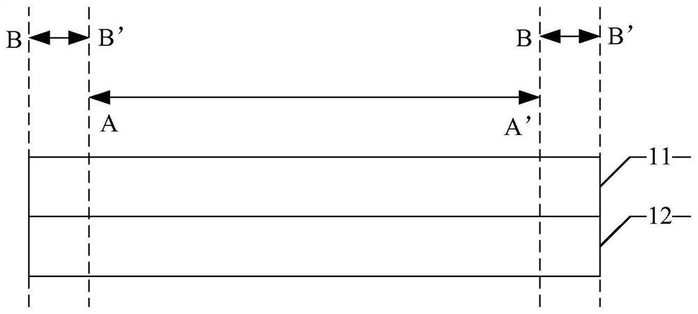
[0039] refer to figure 2 , figure 2 It i...


PUM


Abstract

The invention provides a display panel, a manufacturing method and electronic equipment. The display panel is provided with a display area and a frame area surrounding the display area, and the display panel comprises an array substrate and a glass cover plate which are oppositely arranged; at least two packaging material layers arranged between the array substrate and the glass cover plate, wherein at least two packaging material layers are located in the frame area; and a conductive layer which is arranged between two adjacent packaging structure layers and is connected with a fixed potential. According to the display panel, the packaging material layers are arranged in a layered mode, under the condition that the relative distance between the array substrate and the glass cover plate isnot changed, the thickness of each packaging material layer is small, in this way, in the laser sintering process, the laser sintering effect can be better; in addition, the conducting layers are arranged between every two adjacent packaging material layers, so the static electricity can be guided out in time, each packaging material layer cannot be damaged, the antistatic capacity of the displaypanel is improved to a great extent, and the packaging stability of the display panel is higher.

Description

technical field [0001] The present invention relates to the technical field of OLED, and more particularly, to a display panel, a manufacturing method and an electronic device. Background technique [0002] Organic Light Emitting Diode (OLED), because of its low energy consumption, high resolution, high brightness, high luminous efficiency, fast response speed, wide viewing angle, no need for backlight, low cost and low driving voltage, etc. It has a wide range of research and application prospects in the fields of display and light sources. [0003] However, after the current small-sized OLED panel is packaged with the glass cover plate and the array substrate, during the ESD (Electro-Static Discharge, electrostatic discharge) test, the static electricity cannot be effectively exported, resulting in the packaging of the glass cover plate and the array. The encapsulation structure of the substrate is damaged, thereby affecting the encapsulation stability of the small-sized ...

Claims


Application Information

Patent Timeline
IPC IPC(8): H01L23/60H01L51/52H01L51/56
CPCH01L23/60H10K50/844H10K71/00
Inventor 魏启兵陈敏刘昕昭
Owner SHANGHAI TIANMA AM OLED
Why Eureka
Try Eureka