Chip test information display method and device, electronic equipment and storage medium

A chip testing and chip technology, applied in electrical digital data processing, error detection/correction, detection of faulty computer hardware, etc., can solve problems such as large size, unintuitive chip test results, messy data structure relationships, etc., to achieve intuitive viewing. Effect

Pending Publication Date: 2021-04-06
HYGON INFORMATION TECH CO LTD
View PDF5 Cites 2 Cited by
  • Summary
  • Abstract
  • Description
  • Claims
  • Application Information

AI Technical Summary

Problems solved by technology

[0003] However, the semiconductor chip test files used in the above tests contain a huge amount of information, and there are dependencies in the data

Method used


Image

  • Chip test information display method and device, electronic equipment and storage medium
  • Chip test information display method and device, electronic equipment and storage medium
  • Chip test information display method and device, electronic equipment and storage medium

Examples


Embodiment Construction

[0025] Embodiments of the present invention will be described in detail below in conjunction with the accompanying drawings.

[0026] It should be clear that the described embodiments are only some of the embodiments of the present invention, not all of them. Based on the embodiments of the present invention, all other embodiments obtained by persons of ordinary skill in the art without creative efforts fall within the protection scope of the present invention.

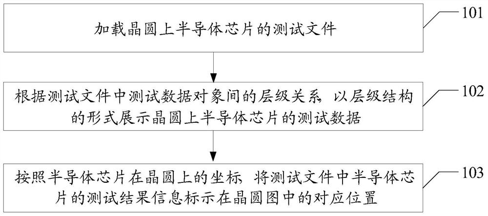
[0027] An embodiment of the present invention provides a chip test information display method, which can be executed by a chip test information display device implemented by software and / or hardware. see figure 1 , the chip test information display method specifically includes the following steps 101-103.

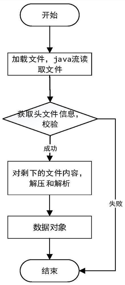
[0028] Step 101, loading the test file of the semiconductor chip on the wafer.

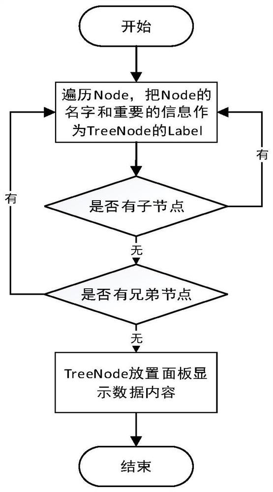
[0029] Step 102: Display the test data of the semiconductor chips on the wafer in a hierarchical structure according to the hierar...


PUM


Abstract

The embodiment of the invention discloses a chip test information display method and device, electronic equipment and a storage medium, relates to the technical field of semiconductor chips, and can overcome the defects of messy chip test data structure relationship and non-intuitive test result in the prior art. The method comprises the following steps: loading a test file of a semiconductor chip on a wafer; displaying the test data of the semiconductor chip on the wafer in a hierarchical structure form according to the hierarchical relationship among the test data objects in the test file; and marking the test result information of the semiconductor chip in the test file at the corresponding position in the wafer diagram according to the coordinates of the semiconductor chip on the wafer. The invention is suitable for a scene of how to visually and clearly present the chip test information.

Description

technical field [0001] The invention relates to the technical field of semiconductor chips, in particular to a chip test information display method, device, electronic equipment and storage medium. Background technique [0002] With the rapid development of computer technology, electronic equipment has become a necessary tool for people's daily work and life. As an indispensable component in electronic equipment, integrated circuits play an extremely important role. Wafer manufacturing is the process of making integrated circuit components on a silicon wafer. After the fabrication is completed, semiconductor chips (Die) arranged in an array are formed on the wafer, and then the wafer is tested to determine the quality level of each chip on it. The distinction, and then pick out the unqualified chips. [0003] However, the semiconductor chip test files used in the above tests contain a huge amount of information, and there are dependencies in the data structure. If the data...

Claims


Application Information

Patent Timeline
IPC IPC(8): G06F16/16G06F11/22
CPCG06F16/168G06F11/2268G06F11/2236Y02P90/30
Inventor 江华张珩陆毅
Owner HYGON INFORMATION TECH CO LTD
Why Eureka
Try Eureka