Display substrate, preparation method thereof and display device

A display substrate and display area technology, which is applied in semiconductor/solid-state device components, semiconductor/solid-state device testing/measurement, semiconductor devices, etc., and can solve problems such as inability to accurately reflect the actual characteristics of transistors in the display area

Pending Publication Date: 2021-10-26
BOE TECH GRP CO LTD +1
View PDF0 Cites 0 Cited by
  • Summary
  • Abstract
  • Description
  • Claims
  • Application Information

AI Technical Summary

Problems solved by technology

[0005] The technical problem to be solved by the present disclosure is to provide a display substrate and its preparation method, and a display device, so as to solve the problem that the existing test components cannot accurately reflect the actual characteristics of the transistors in the display area

Method used


Image

  • Display substrate, preparation method thereof and display device
  • Display substrate, preparation method thereof and display device
  • Display substrate, preparation method thereof and display device

Examples


Embodiment Construction

[0080] In order to make the purpose, technical solution and advantages of the present disclosure clearer, the embodiments of the present disclosure will be described in detail below in conjunction with the accompanying drawings. Note that an embodiment may be embodied in many different forms. Those skilled in the art can easily understand the fact that the means and contents can be changed into various forms without departing from the gist and scope of the present disclosure. Therefore, the present disclosure should not be interpreted as being limited only to the contents described in the following embodiments. In the case of no conflict, the embodiments in the present disclosure and the features in the embodiments can be combined arbitrarily with each other.

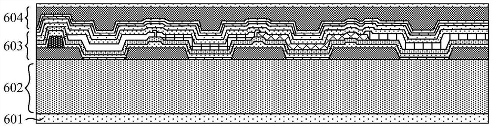
[0081] In the drawings, the size of each component, the thickness of a layer, or a region is sometimes exaggerated for the sake of clarity. Therefore, one aspect of the present disclosure is not necessarily limited to...


PUM


Abstract

The invention provides a display substrate, a preparation method thereof and a display device. The display substrate comprises an effective area and a frame area, the effective area comprises a display area and at least one test area, the display area comprises a plurality of sub-pixels, the at least one sub-pixel comprises a pixel driving circuit, the test area comprises at least one test unit, and the test unit comprises a test transistor, a plurality of test leads and a plurality of test terminals. The structure of the test transistor is the same as that of at least one transistor in the pixel driving circuit, and the plurality of test terminals are connected with the test transistor through the plurality of test leads; the frame area is provided with a plurality of test pins and a plurality of connecting lines, and the plurality of test pins are correspondingly connected with the plurality of test terminals through the plurality of connecting lines. The test circuit is formed in the effective area, the characteristics of the test transistor in the test circuit are basically consistent with the characteristics of the corresponding transistor in the display area, and the test transistor can accurately reflect the actual characteristics of the transistor in the display area.

Description

technical field [0001] The present disclosure relates to but is not limited to the field of display technology, especially to a display substrate, a manufacturing method thereof, and a display device. Background technique [0002] Organic Light Emitting Diode (OLED) is an active light-emitting display device, which has the advantages of self-illumination, wide viewing angle, high contrast, low power consumption, high response speed, light and thin, bendable and low cost. With the continuous development of display technology, a flexible display device (Flexible Display) which uses OLED as a light-emitting device and is signal-controlled by a Thin Film Transistor (TFT) has become a mainstream product in the display field. [0003] The inventors of the present application found that the test components on the existing OLED display substrate cannot accurately reflect the actual characteristics of the transistors in the display area. Contents of the invention [0004] The foll...

Claims


Application Information

Patent Timeline
Patent Type & Authority Applications(China)
IPC IPC(8): H01L27/32H01L23/544
CPCH01L22/34H01L22/32H10K59/00H10K59/123H10K59/1315H10K59/1213H10K59/122
Inventor 李孟
Owner BOE TECH GRP CO LTD
Why Eureka
Try Eureka