Method for making mask read-only memory
A manufacturing method and mask read-only technology, which can be used in semiconductor/solid-state device manufacturing, electrical solid-state devices, semiconductor devices, etc., and can solve problems such as difficulties
- Summary
- Abstract
- Description
- Claims
- Application Information
AI Technical Summary
Problems solved by technology
Method used
Image

Examples
Embodiment Construction
[0037] Preferred embodiments of the present invention will be described in detail below with reference to the accompanying drawings.
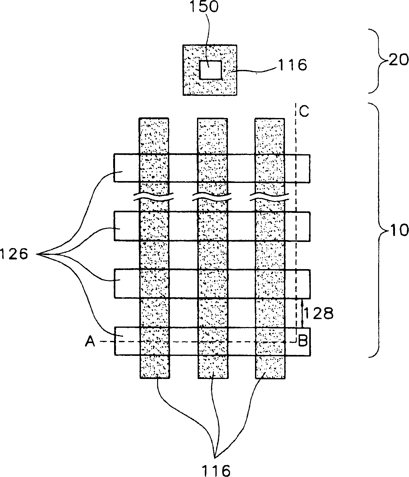
[0038] Figure 4 It is the design diagram of the memory cell array of the present invention.
[0039] When making the mask ROM of the flat cell type of the present invention, as Figure 4 As shown, the element isolation film (not shown) is not separately subjected to LOCOS or STI process for isolating memory cells, but is formed on the periphery of the memory cell array region 30 and has a structure surrounding the entire memory cell array region 30 . In addition, the source / drain (not shown) of the memory cell becomes the buried layer 216 formed before the gate formation process. The contact hole 250 opposite to the buried layer does not exist in the memory cell array region 30 but exists only in the segment selection region 40 . A gate 226 is formed in a direction perpendicular to the buried layer 216 .
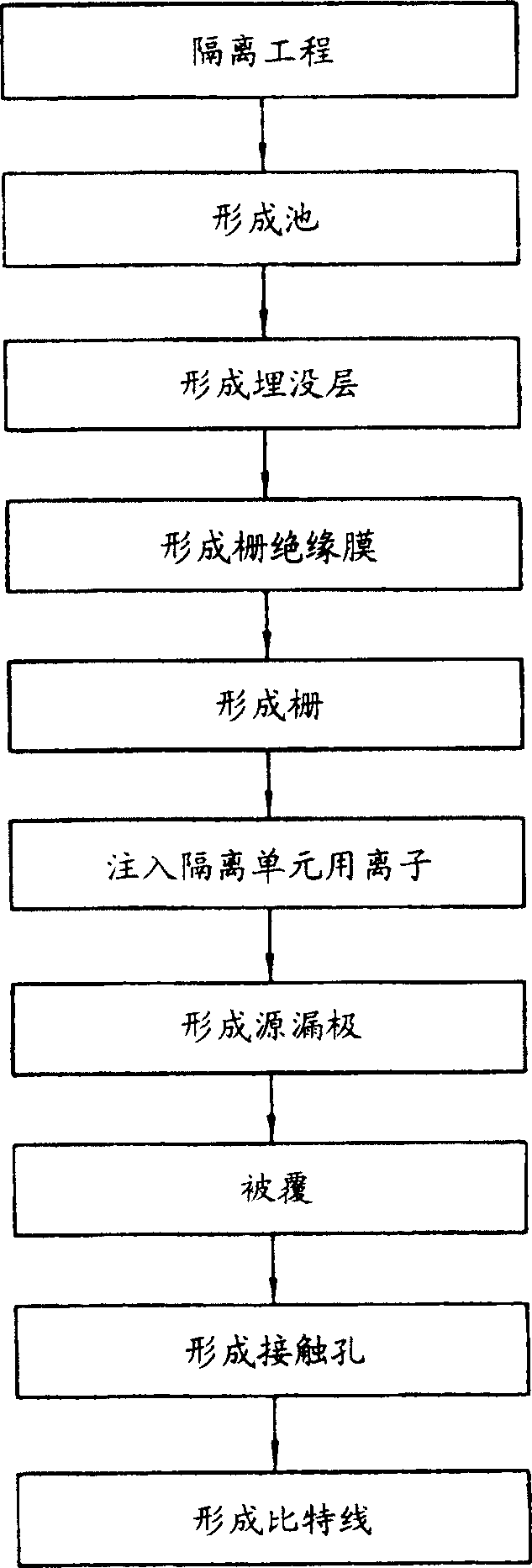
[0040] Figures 5a to 5g are along...
PUM
 Abstract
Description
Claims
Application Information