Check patentability & draft patents in minutes with Patsnap Eureka AI!

Structure, method and system for measuring RIE lag depth

a technology of reactive ions and lag depth, applied in the direction of individual semiconductor device testing, semiconductor/solid-state device testing/measurement, instruments, etc., can solve the problems of reducing the etching rate, affecting the control of deep trench side wall passivation, and affecting the etching ra

Active Publication Date: 2020-06-09
GLOBALFOUNDRIES U S INC
View PDF3 Cites 0 Cited by
  • Summary
  • Abstract
  • Description
  • Claims
  • Application Information

AI Technical Summary

Benefits of technology

Enables accurate identification of RIE lag depth and electrical shorts without destructive testing, using less expensive electrical measurements, thus improving semiconductor device reliability and reducing analysis costs.

Problems solved by technology

With the requirement of scaling, the control of deep trench side wall passivation has become a fundamental issue and an impediment in achieving deeper trenches.
However, the presence of a thick passivation film on the entire inner surface of the deep trench during the etch process leads to a significantly slower etch rate.
Due to misprocessing, poor process setup, etc., RIE lag can cause wide width metal to short to underlying metal even though smaller width metal have depths that are on target and are not shorted.

Method used


Image

  • Structure, method and system for measuring RIE lag depth
  • Structure, method and system for measuring RIE lag depth
  • Structure, method and system for measuring RIE lag depth

Examples


Embodiment Construction

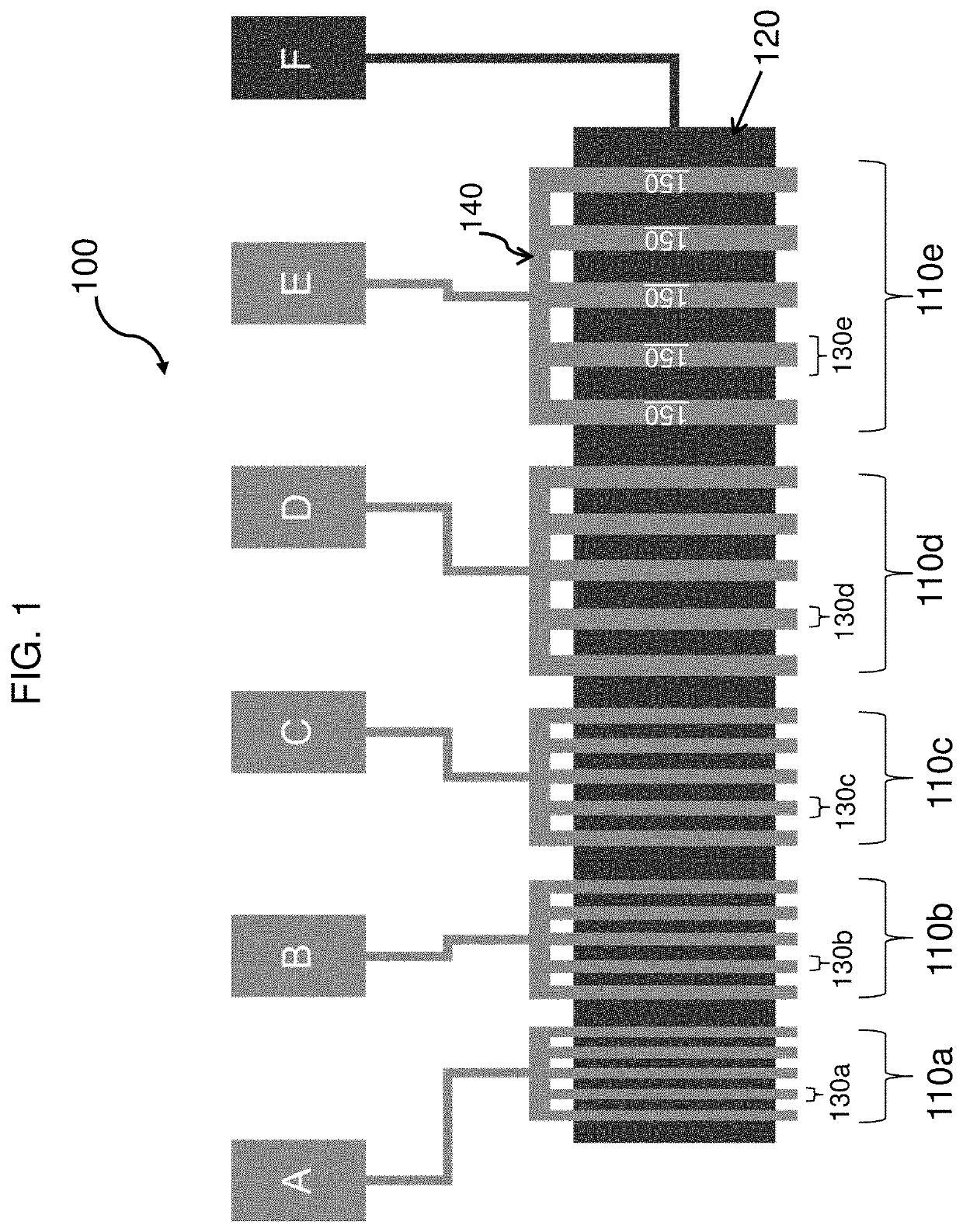
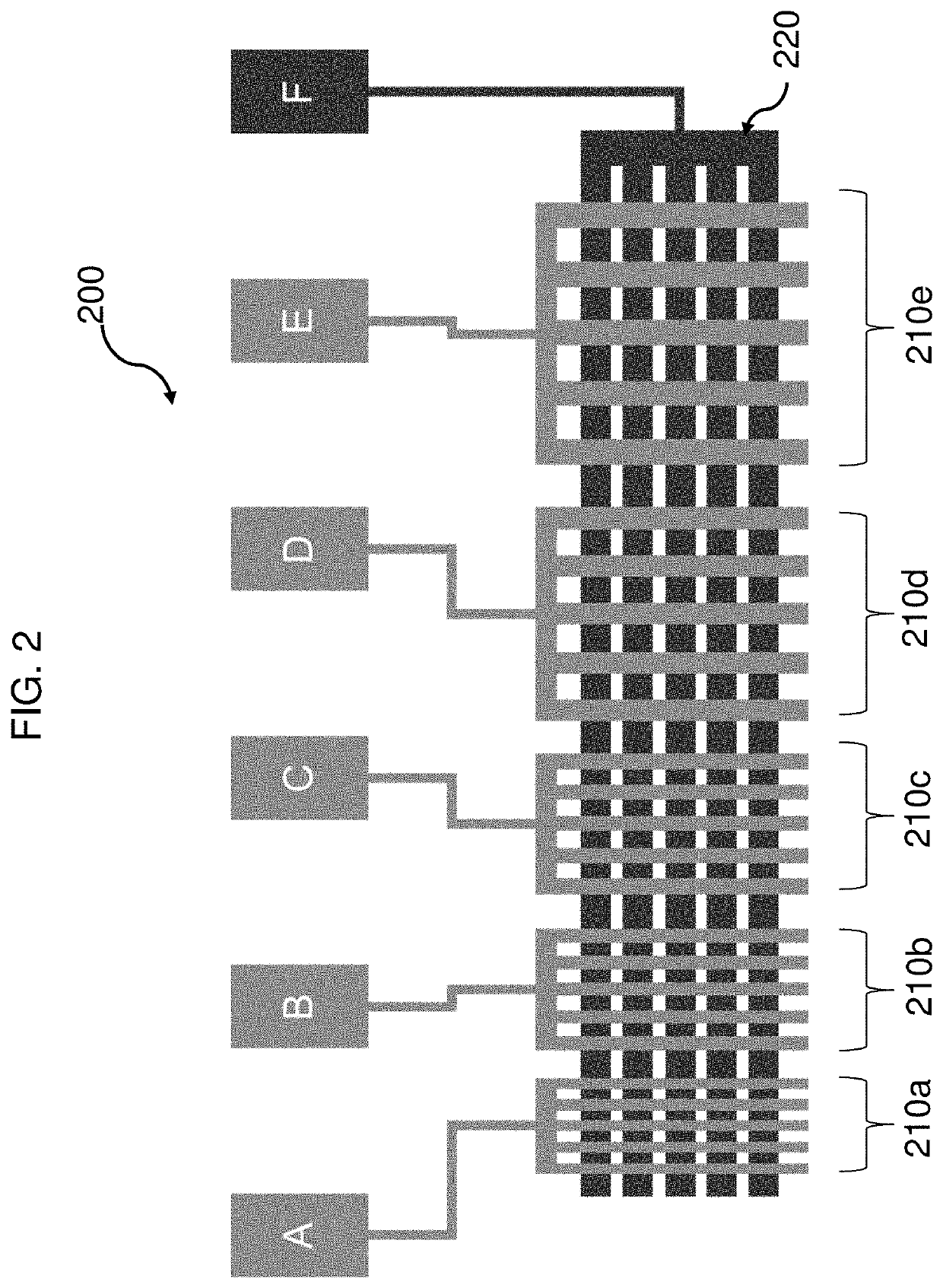
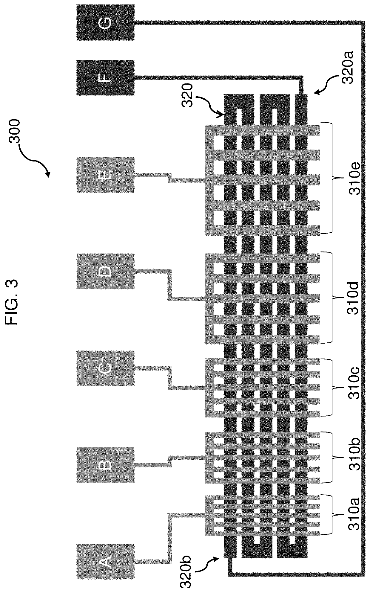
[0017]The subject matter disclosed herein relates to reactive ion etching (RIE) lag depth of semiconductor devices. More specifically, various aspects described herein relate to structures, methods and systems for measuring RIE lag depth and identifying electrical shorts of semiconductor devices.

[0018]As noted above, RIE lag can cause wide width wires to short to underlying metal even though smaller width wires have depths on target that do not short. Typically, expensive and / or destructive analysis techniques are required to determine the cause of a short (a type of failure).

[0019]The structures, methods and systems of the disclosure provide for measuring RIE lag depth and identifying the existence of an electrical short caused by unacceptable RIE lag in a less expensive and non-destructive manner. More specifically, the structures, methods and systems of the disclosure utilize less expensive electrical measuring techniques that do not destroy (e.g., require cutting) the semiconduc...


PUM

PropertyMeasurementUnit
widthaaaaaaaaaa
angleaaaaaaaaaa
widthsaaaaaaaaaa

Abstract

Structures for measuring RIE lag depth of a semiconductor device, including: a first metal layer; a dielectric cap layer on top of the first metal layer; an electrical ground element formed beneath one or more portions of the dielectric cap layer and within the first metal layer, the electrical ground element being electrically grounded; and a second metal layer on top of the dielectric cap layer, the second metal layer having an array of one or more sub-arrays of metal wires, each sub-array being connected to a respective bond pad and having metal wires of a given width; wherein a distance from a bottom surface of the array of metal wires to a top surface of the dielectric cap layer is indicative of RIE lag depth. The disclosure also relates to methods and systems for measuring RIE lag depth and identifying the existence of an electrical short of a semiconductor device.

Description

TECHNICAL FIELD[0001]The subject matter disclosed herein relates to reactive ion etching (RIE) lag depth for semiconductor devices. More specifically, various aspects described herein relate to structures, methods and systems for measuring RIE lag depth and identifying the existence of electrical shorts of semiconductor devices.BACKGROUND[0002]The fabrication of deep trenches in semiconductor dielectrics is one method of making metallic wires, referred to as interconnects. A deep trench of somewhat trapezoidal shape is etched out of a dielectric layer by a commonly used dry etch method known as reactive ion etching (RIE). There is today an ever increasing need to make the deep trenches more narrow to conserve space on the substrate and, hence, to increase productivity. This reduction process is commonly referred to as scaling. The direct result of scaling is that the width of the deep trench ends up substantially reduced. In order to maximize the cross-sectional area of the intercon...

Claims


Application Information

Patent Timeline
Patent Type & Authority Patents(United States)
IPC IPC(8): G01R31/50H01L21/311H01L21/768H01L23/522H01L23/544G01R31/28H01L21/3065H01L21/3213H01L23/532H01L21/66H01L23/528G01R31/26
CPCH01L22/32H01L23/5286H01L22/12G01R31/2601G01R31/2856H01L21/32136H01L21/31116H01L21/76816G01R31/50H01L21/76877H01L23/544H01L21/31138H01L21/3065H01L22/34H01L23/53242H01L23/5329H01L23/53214H01L23/53209H01L23/5226H01L22/14H01L23/53257H01L23/53228
Inventor LICAUSI, NICHOLAS V.
Owner GLOBALFOUNDRIES U S INC
Features
  • R&D
  • Intellectual Property
  • Life Sciences
  • Materials
  • Tech Scout
  • Unparalleled Data Quality
  • Higher Quality Content
  • 60% Fewer Hallucinations
Learn More