Pixel driving circuit and display panel

a driving circuit and display panel technology, applied in the field of display technologies, can solve the problems of short light-emitting time of light-emitting devices thereof, difficult operation of the compensation structure of the oled pixel driving circuit, and relatively complicated operation of the compensation structure of the pixel driving circuit, etc., and achieve low operation difficulty and effective compensation of a threshold voltage

Active Publication Date: 2021-11-09
SHENZHEN CHINA STAR OPTOELECTRONICS SEMICON DISPLAY TECH CO LTD
View PDF3 Cites 3 Cited by
  • Summary
  • Abstract
  • Description
  • Claims
  • Application Information

AI Technical Summary

Benefits of technology

[0003]An object of an embodiment of the present disclosure is to provide a pixel driving circuit and a display panel, which can solve technical problems that a compensation structure of a current pixel driving circuit is complicated, an operation thereof is difficult, and light emitting time of a light emitting device thereof is short.
[0024]Beneficial effects of an embodiment of the present disclosure are that, the embodiment provides a pixel driving circuit and a display panel. The pixel driving circuit uses a 7T3C structure to effectively compensate a threshold voltage of a driving transistor in each pixel, a compensation structure of the pixel driving circuit is relatively simple, and operation difficulty is low. Moreover, a light emitting device emits light during a programming phase and an illumination phase, which increases light emitting time of the light emitting device, thereby improving a brightness and a life of the display panel.

Problems solved by technology

At present, the compensation structure of the OLED pixel driving circuit is relatively complicated, an operation thereof is difficult, and light-emitting time of a light emitting device thereof is short.

Method used


Image

  • Pixel driving circuit and display panel
  • Pixel driving circuit and display panel
  • Pixel driving circuit and display panel

Examples


Embodiment Construction

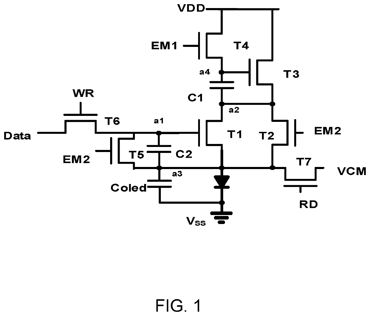
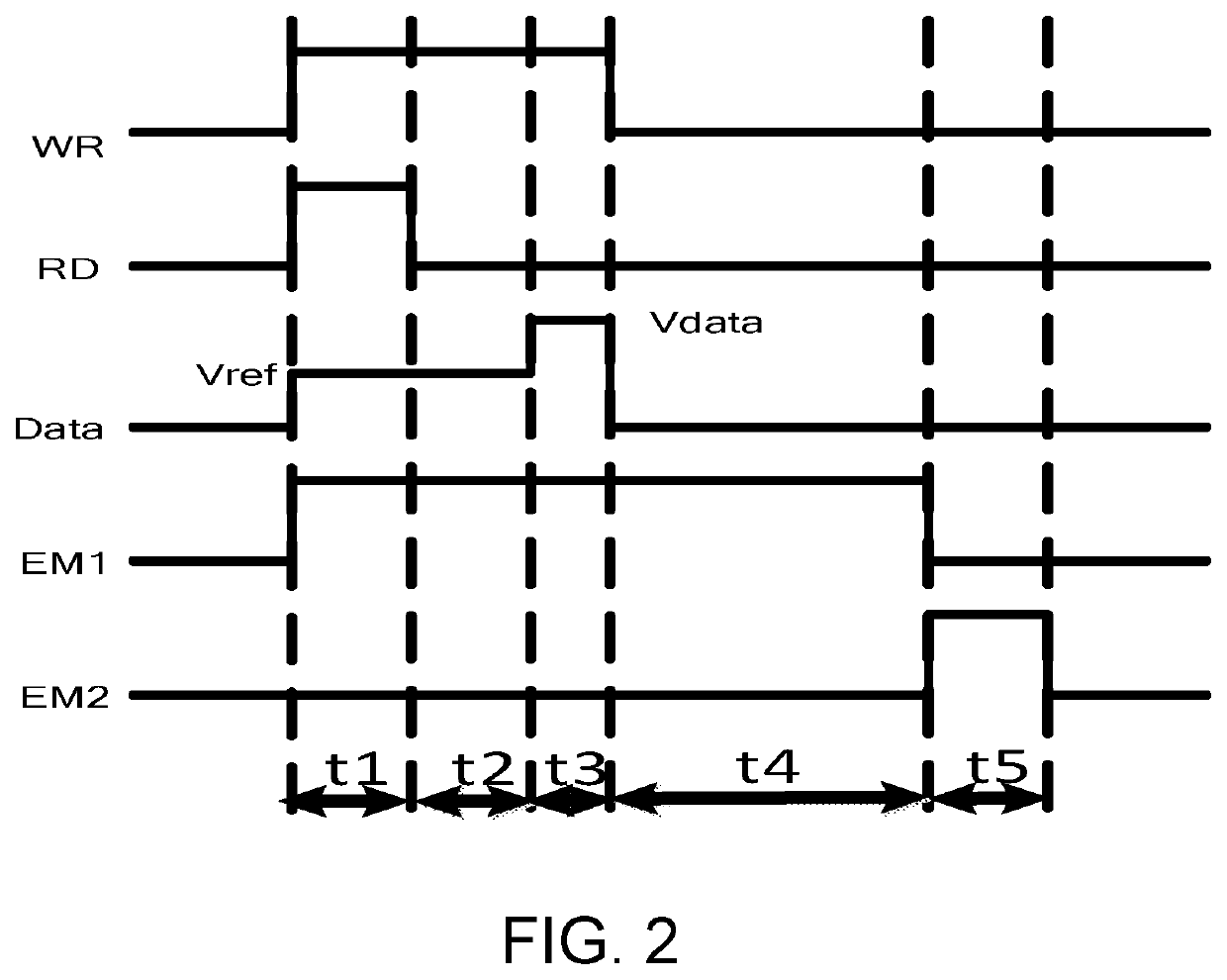
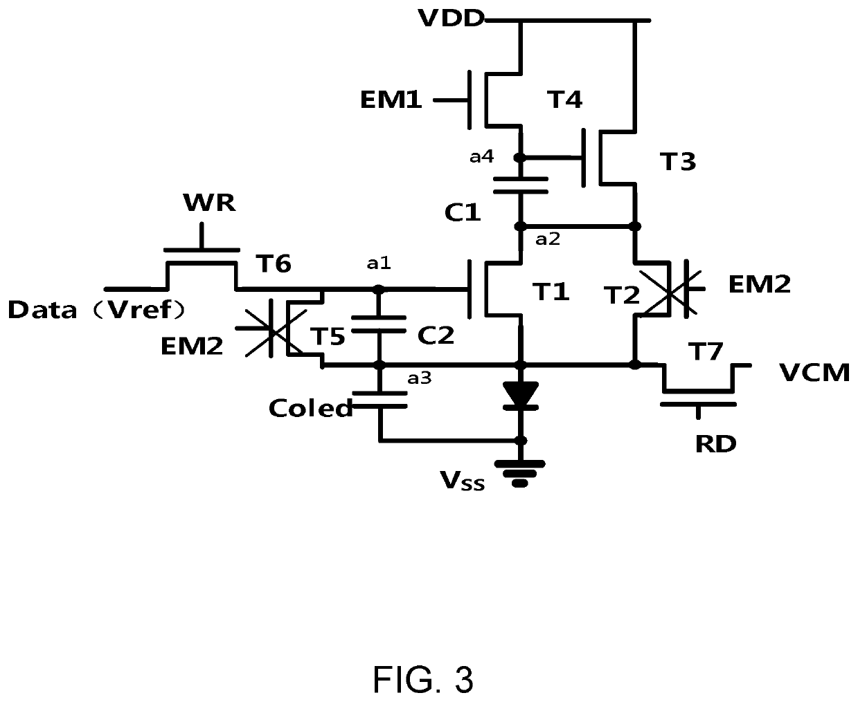
[0033]The technical solutions in the embodiments of the present disclosure will be clearly and completely described in the following with reference to the accompanying drawings in the embodiments. It is apparent that the described embodiments are only a part of the embodiments of the present disclosure, and not all of them. All other embodiments obtained by a person skilled in the art based on the embodiments of the present disclosure without creative efforts are within the scope of the present disclosure.

[0034]Transistors used in all embodiments of the present disclosure may be thin film transistors, field effect transistors, or other devices having the same characteristics. Since sources and drains of the transistors used herein are symmetrical, the sources and the drains are interchangeable. In some embodiments of the present disclosure, in order to distinguish two poles of a transistor except a gate, one of the poles is referred to as a source and the other pole is referred to a...


PUM

PropertyMeasurementUnit
temperatureaaaaaaaaaa
threshold voltageaaaaaaaaaa
thresholdaaaaaaaaaa

Abstract

A pixel driving circuit and a display panel are provided. The pixel driving circuit uses a 7T3C structure to effectively compensate a threshold voltage of a driving transistor in each pixel, a compensation structure of the pixel driving circuit is relatively simple, and operation difficulty is low. Moreover, a light emitting device emits light during a programming phase and an illumination phase, which increases light emitting time of the light emitting device, thereby improving a brightness and a life of the display panel.

Description

FIELD OF INVENTION[0001]The present disclosure relates to the field of display technologies, and more particularly to a pixel driving circuit and a display panel.BACKGROUND OF INVENTION[0002]Organic light emitting diode (OLED) display panels have advantages of high brightness, wide viewing angles, fast response, low power consumption, etc., and have been widely used in the field of high performance display. In the OLED display panel, pixels are arranged in a matrix including a plurality of rows and a plurality of columns, and each pixel is usually composed of two transistors and one capacitor, which is commonly called a 2T1C circuit, the transistor has an issue of threshold voltage drift, therefore, an OLED pixel driving circuit requires a corresponding compensation structure. At present, the compensation structure of the OLED pixel driving circuit is relatively complicated, an operation thereof is difficult, and light-emitting time of a light emitting device thereof is short.SUMMAR...

Claims


Application Information

Patent Timeline
Patent Type & Authority Patents(United States)
IPC IPC(8): G09G3/3225
CPCG09G3/3225G09G2300/043G09G2300/0819G09G2320/0233G09G2320/043G09G3/3208G09G3/3233G09G2300/0823G09G2300/0842G09G2320/045
Inventor NIE, CHENGLEI
Owner SHENZHEN CHINA STAR OPTOELECTRONICS SEMICON DISPLAY TECH CO LTD
Why Eureka
Try Eureka