Light-Emitting Component

a technology of light-emitting components and components, which is applied in the direction of semiconductor lasers, electrical devices, laser details, etc., can solve the problem of inability to direct the light proceeding from the semiconductor laser via the emission opening, and achieve the effect of improving the coupling of light from the first layer into the second layer

Active Publication Date: 2020-04-16
OSRAM OLED
View PDF12 Cites 1 Cited by
  • Summary
  • Abstract
  • Description
  • Claims
  • Application Information

AI Technical Summary

Benefits of technology

[0018]In one embodiment, the interface comprises a rough, uneven structure. A coupling of the light from the first layer into the second layer is improved as a result.
[0019]In one embodiment, in the emission angle range a reflection face is arranged at an inclination with respect to the emission direction of the semiconductor laser, wherein the reflection face deflects the light of the semiconductor laser in the direction of the emission opening. Temporally shorter light pulses may be emitted as a result.

Problems solved by technology

As a result, a direct emission of the light proceeding from the semiconductor laser via the emission opening is not possible.

Method used


Image

  • Light-Emitting Component
  • Light-Emitting Component
  • Light-Emitting Component

Examples


Embodiment Construction

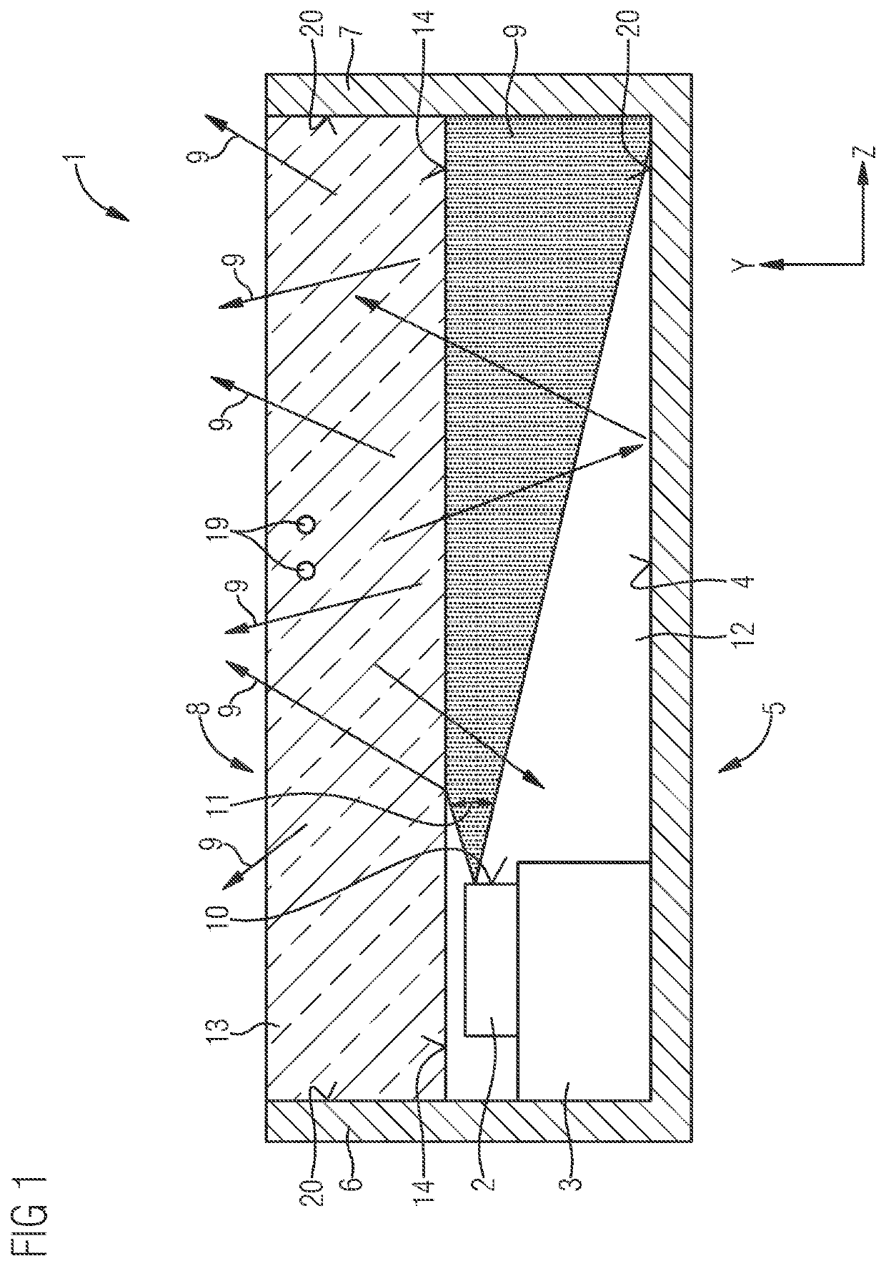
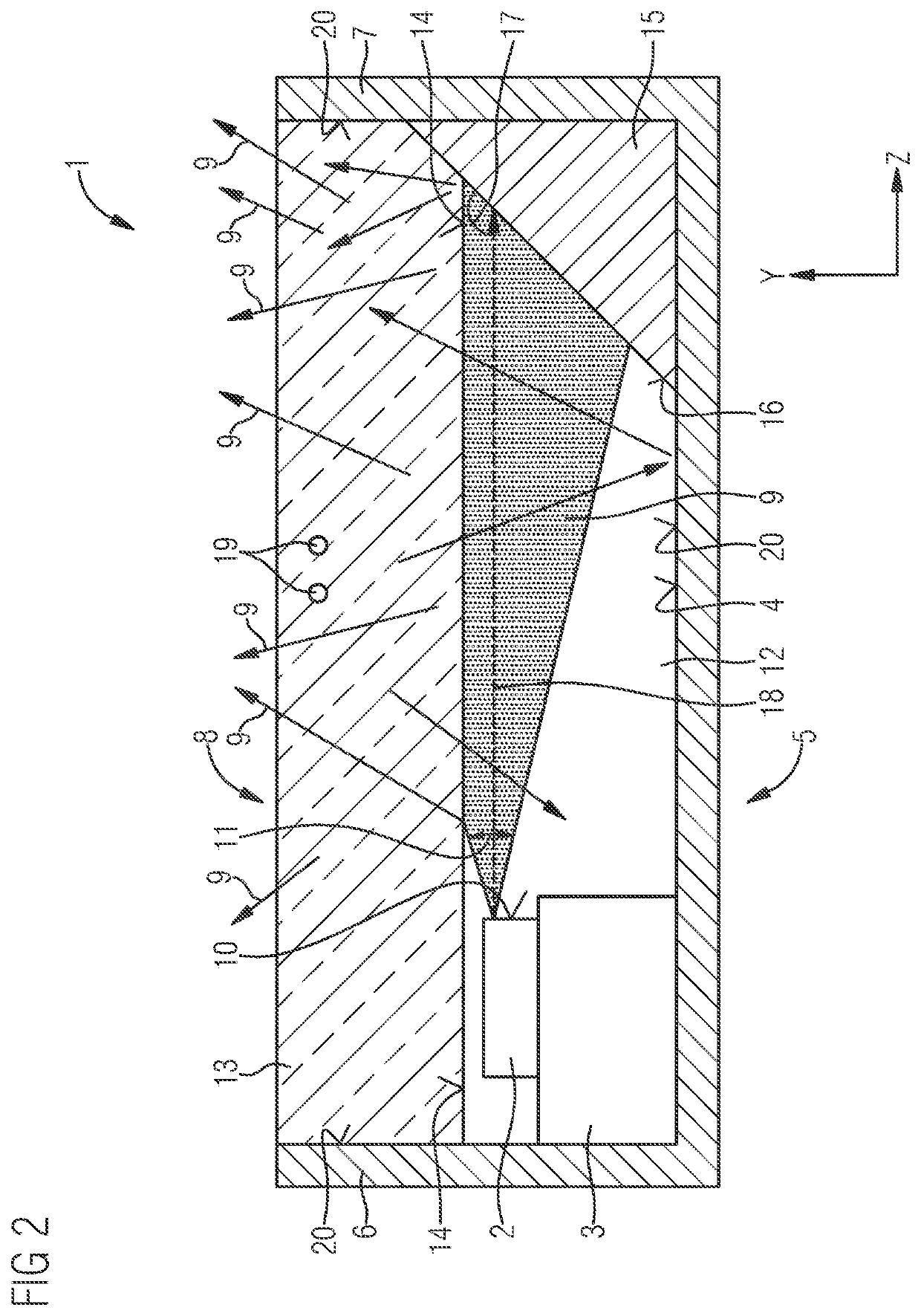
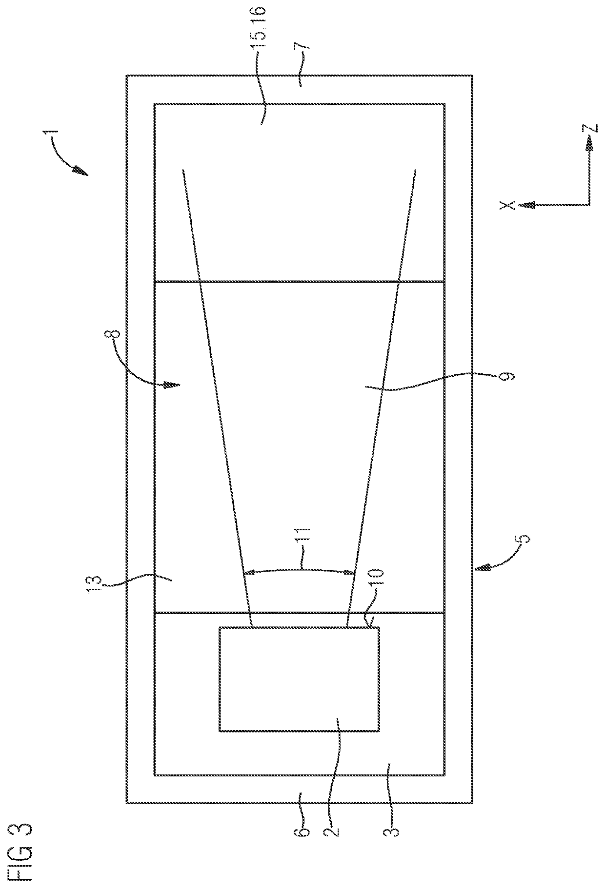
[0024]FIG. 1 shows a schematic cross section through one embodiment of a light-emitting component 1 comprising an edge emitting semiconductor laser 2. The semiconductor laser 2 is arranged on a carrier 3. The carrier 3 may be formed, for example, in the form of a substrate, a leadframe or a ceramic plate. The carrier 3 is secured on a base 4 of a housing 5. The housing 5 comprises four side walls 6, 7 besides the base 4, depending on the embodiment chosen. Moreover, the housing 5 comprises an emission opening 8 for emitting light of the semiconductor laser. In the example illustrated, the emission opening 8 is arranged opposite the base 4. The emission opening 8 may comprise the same area as the base 4 or a smaller area. This is the case, for example, if the housing 5 is covered by a cover plate comprising an opening, wherein the opening constitutes the emission opening. The semiconductor laser 2 emits light 9 at a side face 10. The semiconductor laser 2 may be configured, for examp...


PUM

PropertyMeasurementUnit
angleaaaaaaaaaa
angleaaaaaaaaaa
sizeaaaaaaaaaa

Abstract

In an embodiment a light-emitting component includes a housing and an edge emitting semiconductor laser arranged in the housing, wherein the semiconductor laser is configured to emit light at a side face in an angle range, wherein the housing includes an emission opening for emitting the light, wherein the semiconductor laser is arranged in a first layer having a first material, wherein a second layer is arranged on the first layer, the second layer having a second material, wherein the first layer and the second layer are transmissive to the light, wherein the second layer is arranged between the first layer and the emission opening, wherein the emission opening lies at least partly outside the angle range of the semiconductor laser, and wherein a part of the light is directed directly onto an interface between the first and second layers.

Description

[0001]This patent application is a national phase filing under section 371 of PCT / EP2017 / 058774, filed Apr. 12, 2017, which claims the priority of German patent application 10 2016 106 896.9, filed Apr. 14, 2016, each of which is incorporated herein by reference in its entirety.TECHNICAL FIELD[0002]The invention relates to a light-emitting component.BACKGROUND[0003]A laser diode comprising at least two active layers arranged one above another is described in the prior art, for example, by International Patent Application No. WO 0133607 A2, said laser diode being arranged in an LED housing comprising a radiation-transmissive potting.SUMMARY OF THE INVENTION[0004]Embodiments provide an improved light-emitting component in particular for a time-of-flight measurement.[0005]One advantage of the component described is that the component is constructed in a simple manner, and that the component is suitable for providing short light pulses for one time-of-flight measurement. This advantage ...

Claims


Application Information

Patent Timeline
Patent Type & Authority Applications(United States)
IPC IPC(8): H01S5/022H01S5/0232
CPCH01S5/02292H01S5/02228H01S5/02244H01S5/02216H01S5/02234H01S5/02255H01S5/0232
Inventor HALBRITTER, HUBERTENZMANN, ROLANDWOJCIK, ANDREAS
Owner OSRAM OLED
Why Eureka
Try Eureka