

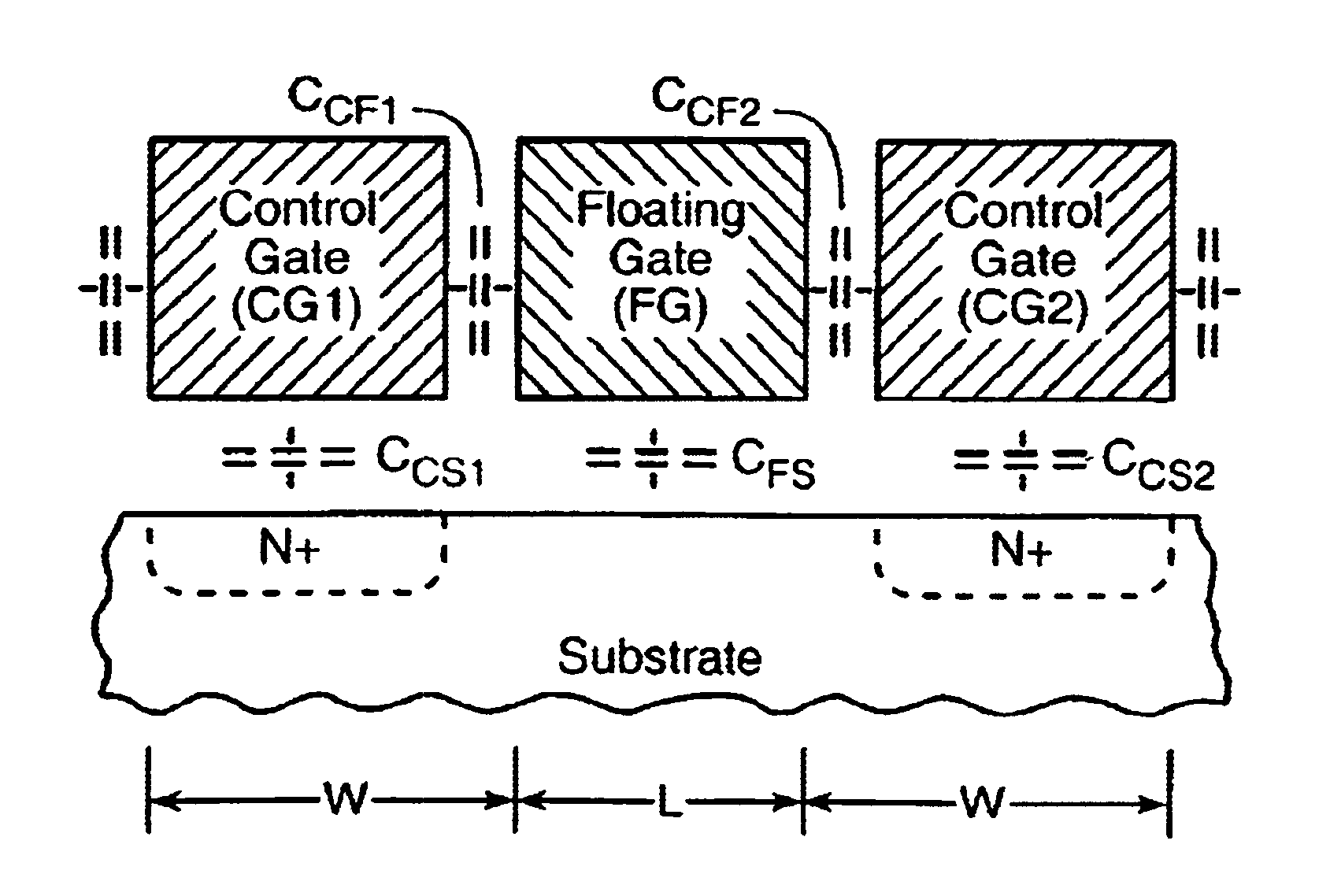
Flash memory cell arrays having dual control gates per memory cell charge storage element
a memory cell array and charge storage technology, applied in semiconductor devices, digital storage, instruments, etc., can solve the problems of difficult long-term data retention, inability to practically be thinned, and significant limitation of the continued shrinkage of the size of current non-volatile memory cell arrays, etc., to increase parasitic capacitance, increase the total coupling area, and increase the coupling ratio
- Summary
- Abstract
- Description
- Claims
- Application Information
AI Technical Summary
Benefits of technology
Problems solved by technology
Method used
Image

Examples
Embodiment Construction
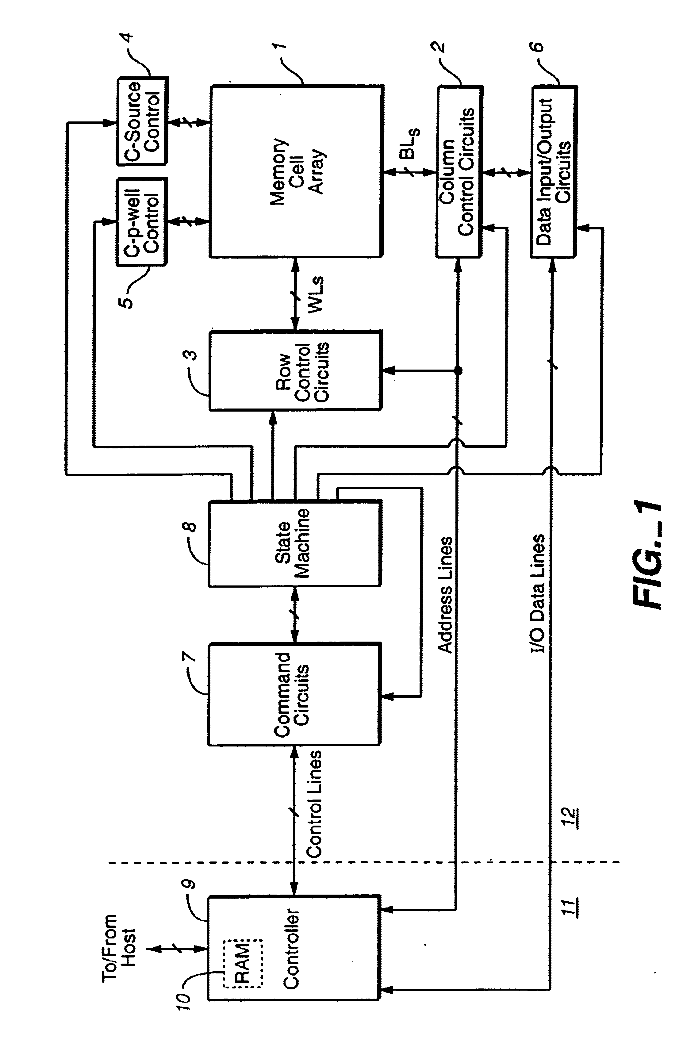
Memory System
[0031]An example memory system in which the various aspects of the present invention may be implemented is illustrated by the block diagram of FIG. 1. A memory cell array 1 including a plurality of memory cells M arranged in a matrix is controlled by a column control circuit 2, a row control circuit 3, a c-source control circuit 4 and a c-p-well control circuit 5. The memory cell array 1 is, in this example, of the NAND type that is described above in the Background and in references incorporated herein by reference. A control circuit 2 is connected to bit lines (BL) of the-memory cell array 1 for reading data stored in the memory cells (M), for determining a state of the memory cells (M) during a program operation, and for controlling potential levels of the bit lines (BL) to promote the programming or to inhibit the programming. The row control circuit 3 is connected to word lines (WL) to select one of the word lines (WL), to apply read voltages, to apply program volt...
PUM
 Abstract
Description
Claims
Application Information