Side-coupled dual-channel optical waveguide transmission system for photonic crystal
A photonic crystal and transmission system technology, applied in the coupling of optical waveguides, light guides, optics, etc., can solve the problems of difficult control of distance parameters between graded optical fibers and photonic crystal devices, the influence of integration, and limitations, and achieve compact structure and high integration. The effect of high degree and simple structure
- Summary
- Abstract
- Description
- Claims
- Application Information
AI Technical Summary
Problems solved by technology
Method used
Image
Examples
specific Embodiment approach 1
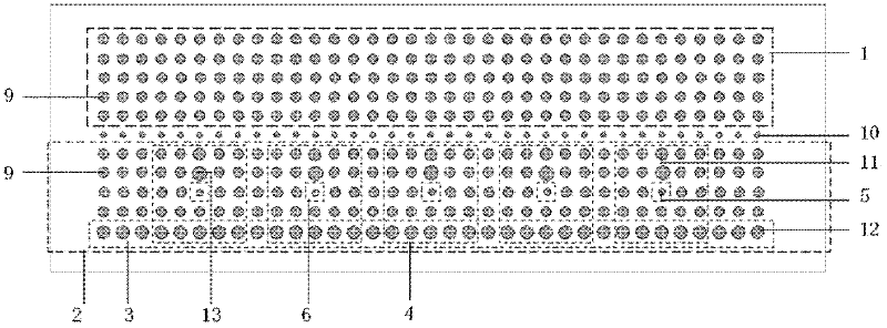
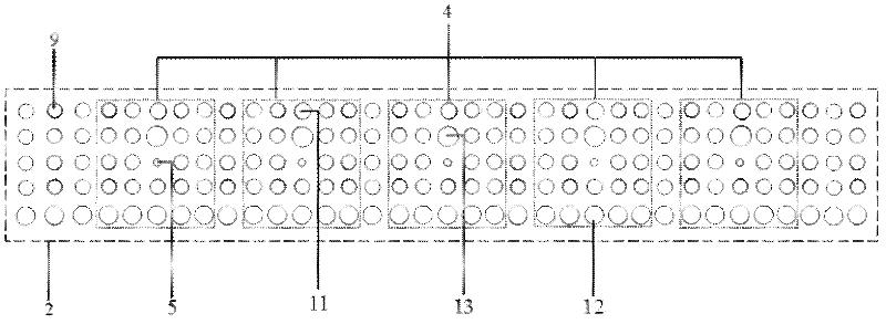
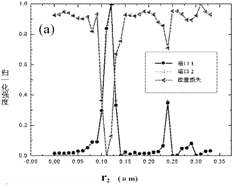
[0018] Specific implementation mode one, combination Figure 1 to Figure 5 In this embodiment, the photonic crystal side-coupled dual-channel optical waveguide transmission system includes a waveguide layer, a low refractive index buried layer 7 and a substrate layer 8. The waveguide layer is located above the low refractive index buried layer 7, and the low refractive index buried layer 7 The lower part is connected to the substrate layer 8; the waveguide layer includes a waveguide first region 1, a defect region, and a waveguide second region 2. The waveguide first region 1 is composed of a plurality of dielectric pillars 9 arranged periodically, the waveguide first region 1 and the waveguide second region A row of defective dielectric pillars 10 is distributed at the junction of 2, and the row of defective dielectric pillars constitutes a defective area. A row of coupling dielectric pillars 12 is distributed on the outermost part of the second waveguide area. This row of coupl...
specific Embodiment approach 2
[0033] Specific implementation mode two, combination Figure 6 to Figure 9 To describe this embodiment, this embodiment is the specific manufacturing process of the photonic crystal side-coupled dual-channel optical waveguide transmission system described in the first embodiment:
[0034] The first step is to prepare the dicing groove required for dicing;
[0035] (A) The substrate silicon 101 is 600 μm thick, on which a 3 μm thick silicon dioxide buried layer 102 is grown (such as Figure 6a (Shown) for cleaning;
[0036] (B) such as Figure 6b As shown, a layer of lanthanum aluminate film 103 is prepared by a sol-gel method on the silicon dioxide buried layer 102;
[0037] (C) such as Figure 6c As shown, a photoresist film 104 with a thickness of 2-3 μm is formed on the lanthanum aluminate film 103;
[0038] (D) Put the completed structure in step (C) into an oven before baking;
[0039] (E) such as Figure 6d As shown, ultraviolet exposure is performed on the photoresist film 104 to ...
PUM
 Abstract
Description
Claims
Application Information


