Touch substrate, fabrication method for touch substrate, and touch apparatus

A substrate and touch technology, which is applied in the fields of instruments, electrical digital data processing, and data processing input/output processes, etc., can solve problems such as unfavorable touch sensitivity and small capacitive coupling area.

Inactive Publication Date: 2016-05-04
BOE TECH GRP CO LTD +1
View PDF6 Cites 5 Cited by
  • Summary
  • Abstract
  • Description
  • Claims
  • Application Information

AI Technical Summary

Problems solved by technology

figure 1 In the structure, the space defined by the receiving electrode pattern 100 in the edge area is small, so the capacitive coupling area between the receiving electrode pattern 100 and the transmitting electrode 210 in this area is also small, which is not conducive to providing touch sensitivity.

Method used


Image

  • Touch substrate, fabrication method for touch substrate, and touch apparatus
  • Touch substrate, fabrication method for touch substrate, and touch apparatus
  • Touch substrate, fabrication method for touch substrate, and touch apparatus

Examples


Embodiment Construction

[0026] The specific implementation manners of the present invention will be further described below in conjunction with the drawings and examples. The following examples are only used to illustrate the technical solution of the present invention more clearly, but not to limit the protection scope of the present invention.

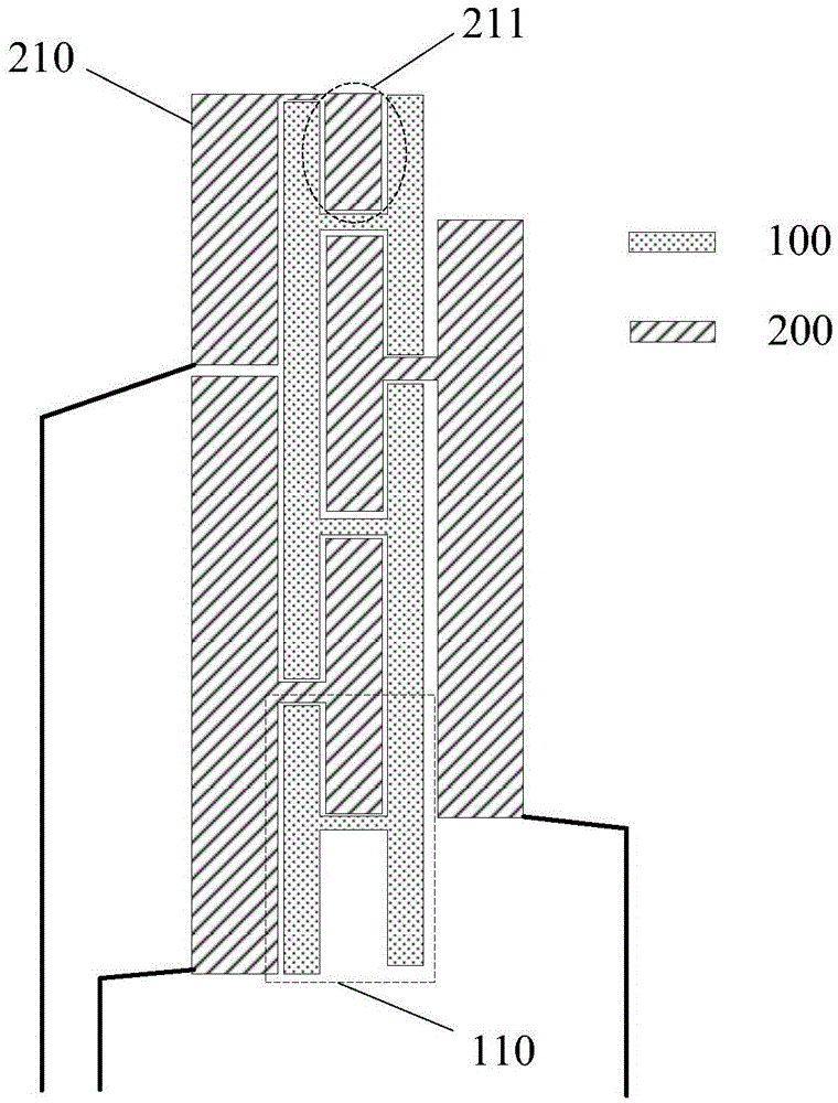
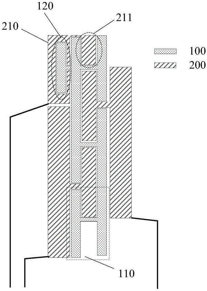
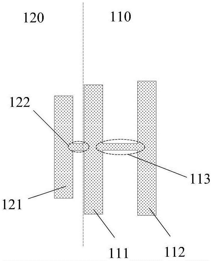
[0027] The structural schematic diagram of the touch substrate provided by an embodiment of the present invention can refer to figure 2 , including a first touch electrode pattern 100 and a second touch electrode pattern 200; wherein the first touch electrode pattern 100 includes a plurality of first touch electrodes 110 and an extended portion 120 at the end; refer to image 3 , is a schematic diagram of the structure of the first touch electrode pattern 100 at the end, including a first touch electrode 110 and a protruding part 120 at this position; wherein, the first touch electrode 110 includes two strip-shaped main parts 111 and 112 and a strip-shape...


PUM


Abstract

The invention provides a touch substrate, a fabrication method for the touch substrate, and a touch apparatus. The touch substrate comprises a substrate as well as a first touch electrode graph and a second touch electrode graph that are formed on the substrate in a same-layer manner. Each second touch electrode comprises a main body part and an extension part; and the extension part of each second touch electrode is correspondingly embedded in a gap of the first touch electrode graph. The first touch electrode graph further comprises an extension part located at the end part and connected to a main body part of a first touch electrode located at the end part; a gap corresponding to the extension part of the first touch electrode graph is formed in the main body part of the second touch electrode located at the end part; and the extension part of the first touch electrode graph is embedded in the gap. According to the touch substrate provided by the invention, the end part coupling area of the second touch electrode graph and the first touch electrode graph can be enlarged, so that the sensitivity of touch detection of a region can be improved.

Description

technical field [0001] The present invention relates to the field of touch technology, in particular to a touch substrate, a manufacturing method thereof, and a touch device. Background technique [0002] In order to reduce the thickness of the display device, a touch device is proposed in the prior art in which the emitter electrode pattern and the receive electrode pattern are made on the same layer. When the finger touches the corresponding area, the gap between the emitter electrode pattern and the receive electrode pattern A change in the capacitance of , which causes a change in the sensed current. see figure 1 , is a structural schematic diagram of a transmitter electrode pattern and a receiver electrode pattern in a touch substrate in the prior art, including a receiver electrode pattern 100 and a transmitter electrode pattern 200; wherein the receiver electrode pattern 100 includes a plurality of aligned receiving electrodes 110, which are relatively The long side...

Claims


Application Information

Patent Timeline
Patent Type & Authority Applications(China)
IPC IPC(8): G06F3/041G06F3/044
CPCG06F3/0412G06F3/044G06F2203/04103G06F2203/04111G06F2203/04112G06F3/0443
Inventor 化磊何剑蔡斯特
Owner BOE TECH GRP CO LTD
Why Eureka
Try Eureka