ION implant monitoring through measurement of modulated optical response

a technology of modulated optical response and implant monitoring, which is applied in the field of optical devices for measuring the concentration of dopant in semiconductor samples, can solve the problems of implantation damage to the crystal lattice, amplitude measurement is no longer well behaved, and damage is typically proportional, and achieves acceptable accuracy.

a technology of modulated optical response and implant monitoring, which is applied in the field of optical devices for measuring the concentration of dopant in semiconductor samples, can solve the problems of implantation damage to the crystal lattice, amplitude measurement is no longer well behaved, and damage is typically proportional, and achieves acceptable accuracy.

US20050083528A1Active Publication Date: 2005-04-21THERMA WAVE INC

Image

  • ION implant monitoring through measurement of modulated optical response
  • ION implant monitoring through measurement of modulated optical response
  • ION implant monitoring through measurement of modulated optical response

Examples


Embodiment Construction

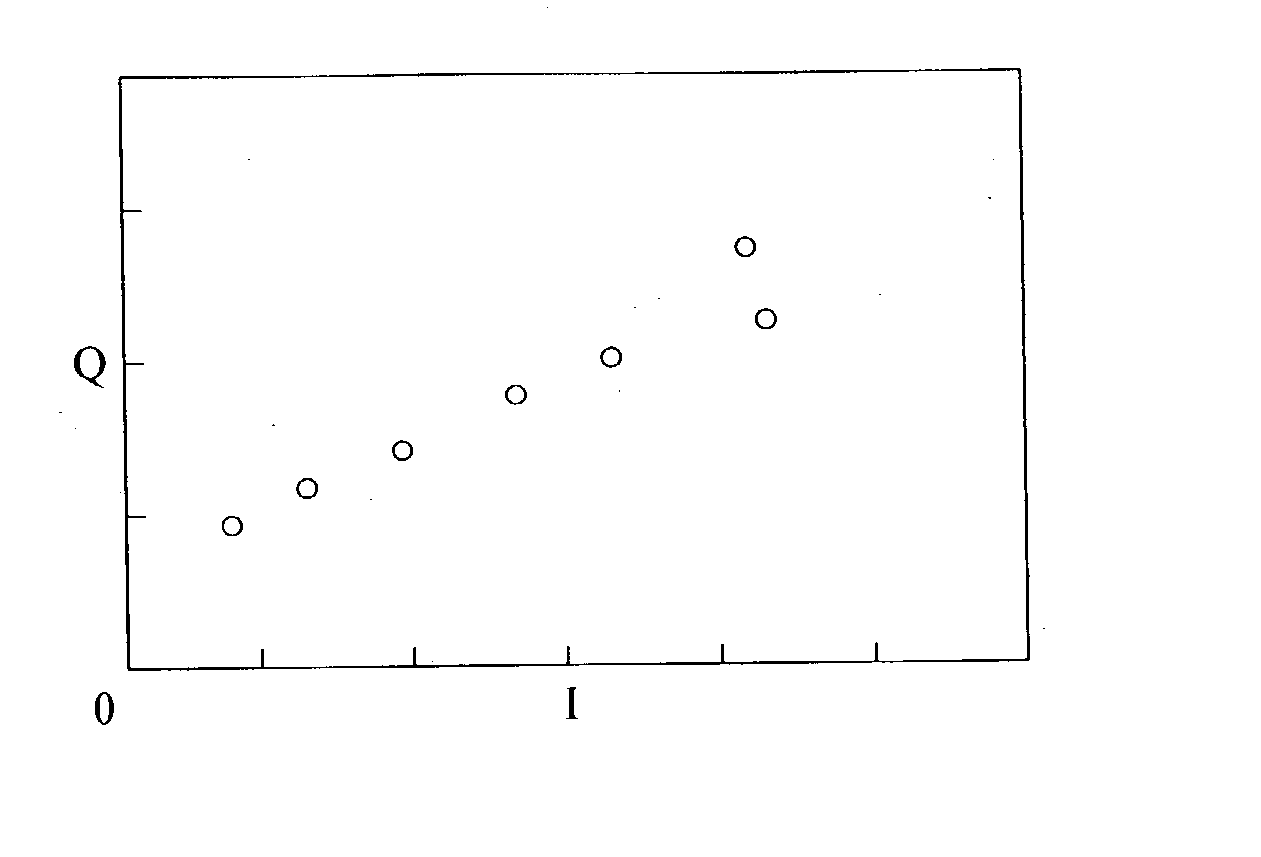
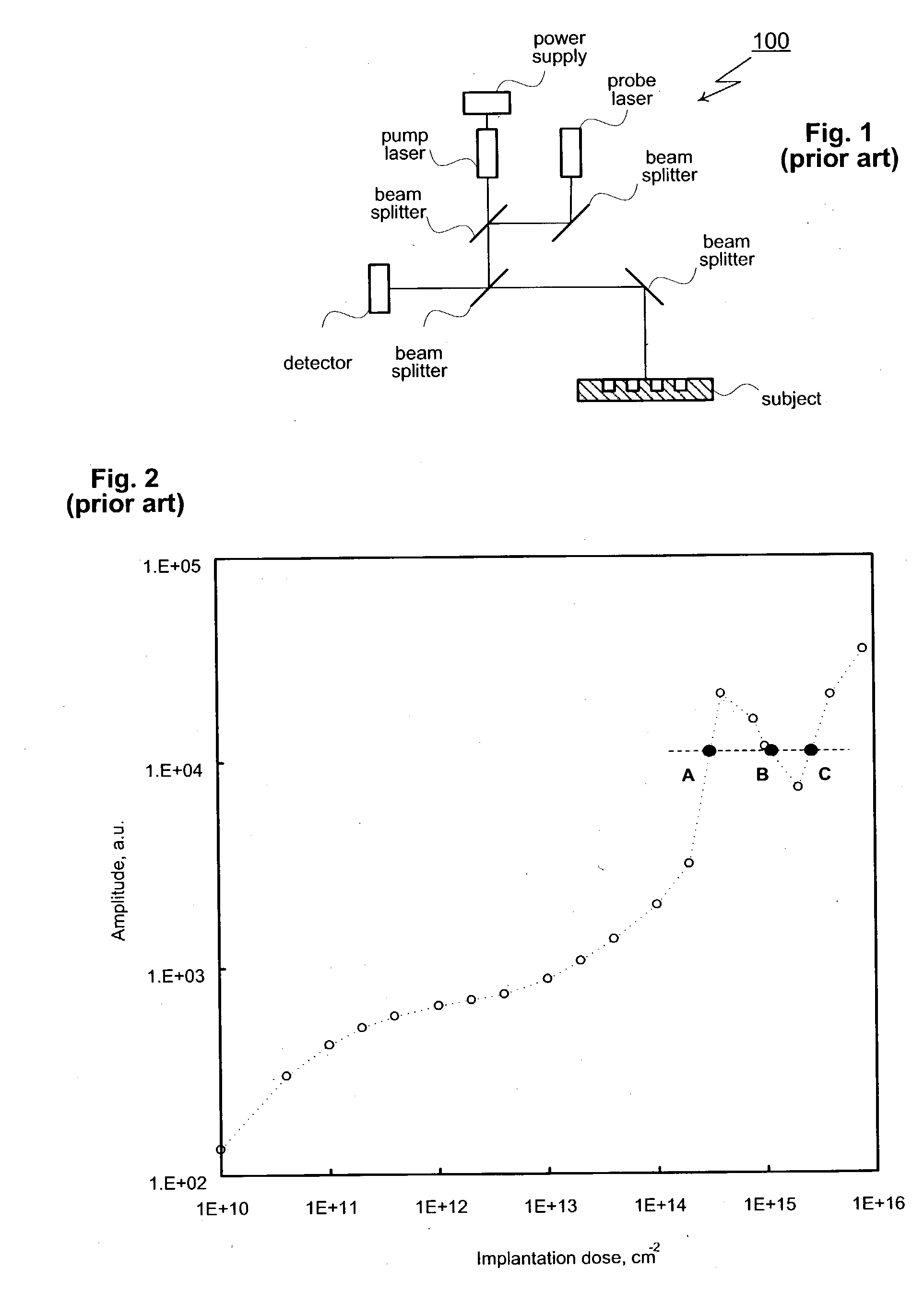
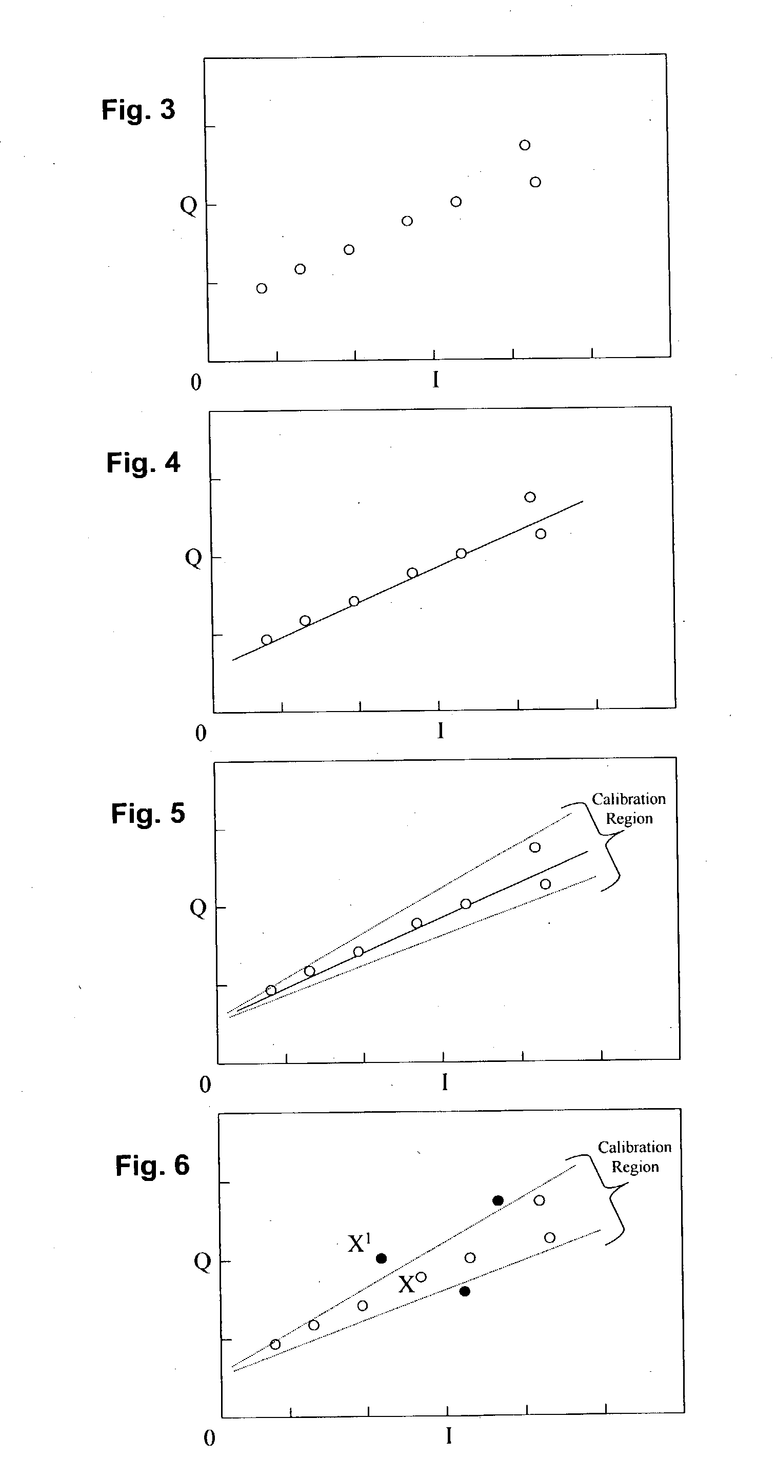
[0025] The present invention provides a method for simultaneously measuring ion implantation dose, damage and / or dopant depth profiles in ion-implanted semiconductors. The measurement method is logically divided into two steps: a calibration and a measurement step. During the calibration step, the photo-modulated reflectance of a known damage profile is characterized. Typically, this involves identifying one or more areas within I-Q space that correspond to the photo-modulated reflectance of the known damage profile. All other areas within I-Q space are then assumed to be dissimilar to the known damage profile. In the measurement step, I-Q measurements for a test subject are obtained empirically. The empirically obtained I-Q measurements are then compared to determine if they fall within an identified region of I-Q space. This comparison indicates whether the test subject has a damage profile that is similar to the known damage profile. The following sections describe several possib...


PUM

PropertyMeasurementUnit
photo-modulated reflectanceaaaaaaaaaa
phase synchronous detectionaaaaaaaaaa
distanceaaaaaaaaaa

Abstract

A method for simultaneously monitoring ion implantation dose, damage and / or dopant depth profiles in ion-implanted semiconductors includes a calibration step where the photo-modulated reflectance of a known damage profile is identified in I-Q space. In a following measurement step, the photo-modulated reflectance of a subject is empirically measured to obtain in-phase and quadrature values. The in-phase and quadrature values are then compared, in I-Q space, to the known damage profile to characterize the damage profile of the subject.

Description

PRIORITY CLAIM [0001] This application claims priority from prior provisional application Ser. Nos. 60 / 365,237, filed Mar. 18, 2002, and 60 / 378,140, filed May 14, 2002, both of which are incorporated herein by reference.TECHNICAL FIELD [0002] The subject invention relates to optical devices used to non-destructively evaluate semiconductor wafers. In particular, the present invention relates to systems for measuring dopant concentrations in semiconductor samples. BACKGROUND OF THE INVENTION [0003] As geometries continue to shrink, manufacturers have increasingly turned to optical techniques to perform non-destructive inspection and analysis of semiconductor wafers. The basis for these techniques is the notion that a subject may be examined by analyzing the reflected energy that results when an optical beam is directed at a subject. This type of inspection and analysis is known as optical metrology and is performed using a range of different optical techniques. [0004] One widely used ...

Claims


Application Information

Patent Timeline
21 Apr 2005
Publication
US20050083528A1
IPC
G01N21/27; G01N21/35; G01N21/55
CPC
G01N21/276; G01N2021/3568; G01N21/55; G01N21/1717
Inventors
SALNIK, ALEX; NICOLAIDES, LENA