Analog floating gate charge loss compensation circuitry and method

a technology of loss compensation circuitry and analog floating gate, which is applied in the direction of electric variable regulation, process and machine control, instruments, etc., can solve the problems of programming accuracy of the amount of charge stored, the loss of charge from the floating gate, and the switch of the stored sta

Active Publication Date: 2013-11-26
TEXAS INSTR INC
View PDF7 Cites 1 Cited by
  • Summary
  • Abstract
  • Description
  • Claims
  • Application Information

AI Technical Summary

Benefits of technology

[0042]It is an object of the invention to provide a circuit and method for compensating loss of trapped charge on a floating gate in an AFG (analog floating gate) circuit.
[0043]It is another object of the invention to provide an inexpensive circuit and method that makes it more practical for precision analog floating gate circuits to retain their accuracy over acceptable circuit lifetimes.
[0044]It is another object of the invention to provide a practical way to avoid the need to provide complex circuitry to compensate for undesired loss of charge from analog floating gates of AFG circuitry.

Problems solved by technology

Some charge may be lost from the floating gate of the EEPROM cell 1, but never enough to switch the stored state.
However, in AFG (analog floating gate) circuit applications, both the programming accuracy of the amount of charge stored on a floating gate and the amount of undesired charge “loss” from the electrically floating gate in an analog circuit application may be problematic because the resulting voltage of the floating gate directly and continuously affects the achievable accuracy of the application circuit in which the floating gate transistor 3 is used.
This, of course, may cause an unacceptable loss in the accuracy of analog circuitry in which floating gate transistor 3 is used.
Consequently, use of the bipolar FNT tunneling technique as used in such structures is not very scalable to present state-of-the-art wafer fabrication processes.
In “nanopower” applications wherein the quiescent current needs to be less than a micrompere, the problem of providing accurate reference voltages is very important and challenging because the resistors of the voltage reference circuits must be very large, and consequently the associated thermal noise becomes unacceptably large.
Conventional bandgap voltage reference circuits for generating accurate reference voltages usually consume substantial amounts of current, because reducing resistor noise in a bandgap voltage reference circuit typically requires increasing the amount of current therein (since the input-referred thermal noise is inversely proportional to the square root of current in the bandgap voltage reference circuit).
This simultaneous conduction approach to programming of floating gate voltages results in accuracy sufficient for precision analog use, but requires some additional process complexity for the tunneling structure.
The minute amount of charge loss during powering up and down of the circuit is insignificant.
It also is believed that the prior art does not disclose passive or active direct compensation for loss of charge the analog floating gates which generally occurs over the product lifetime.

Method used


Image

  • Analog floating gate charge loss compensation circuitry and method
  • Analog floating gate charge loss compensation circuitry and method
  • Analog floating gate charge loss compensation circuitry and method

Examples


Embodiment Construction

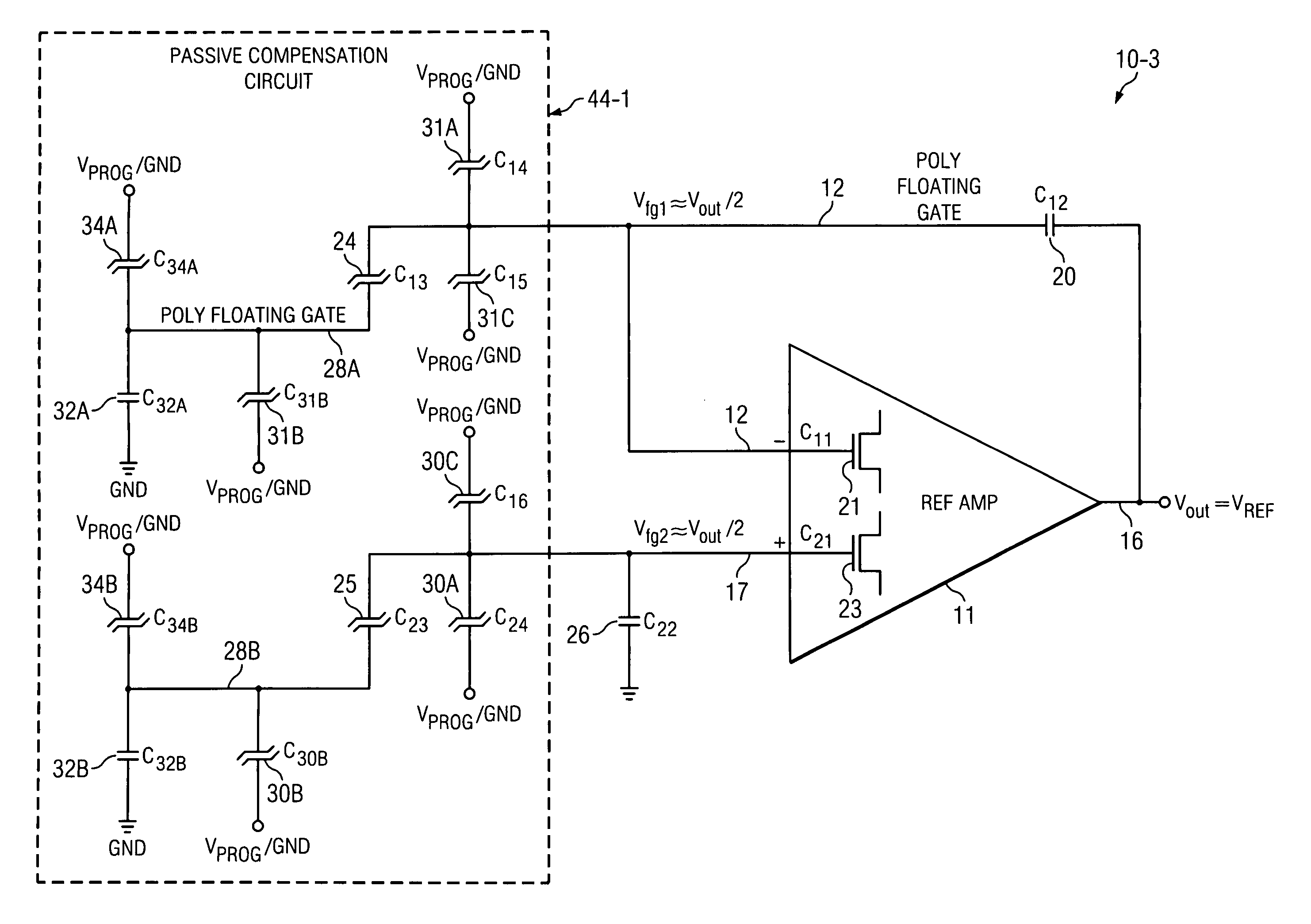
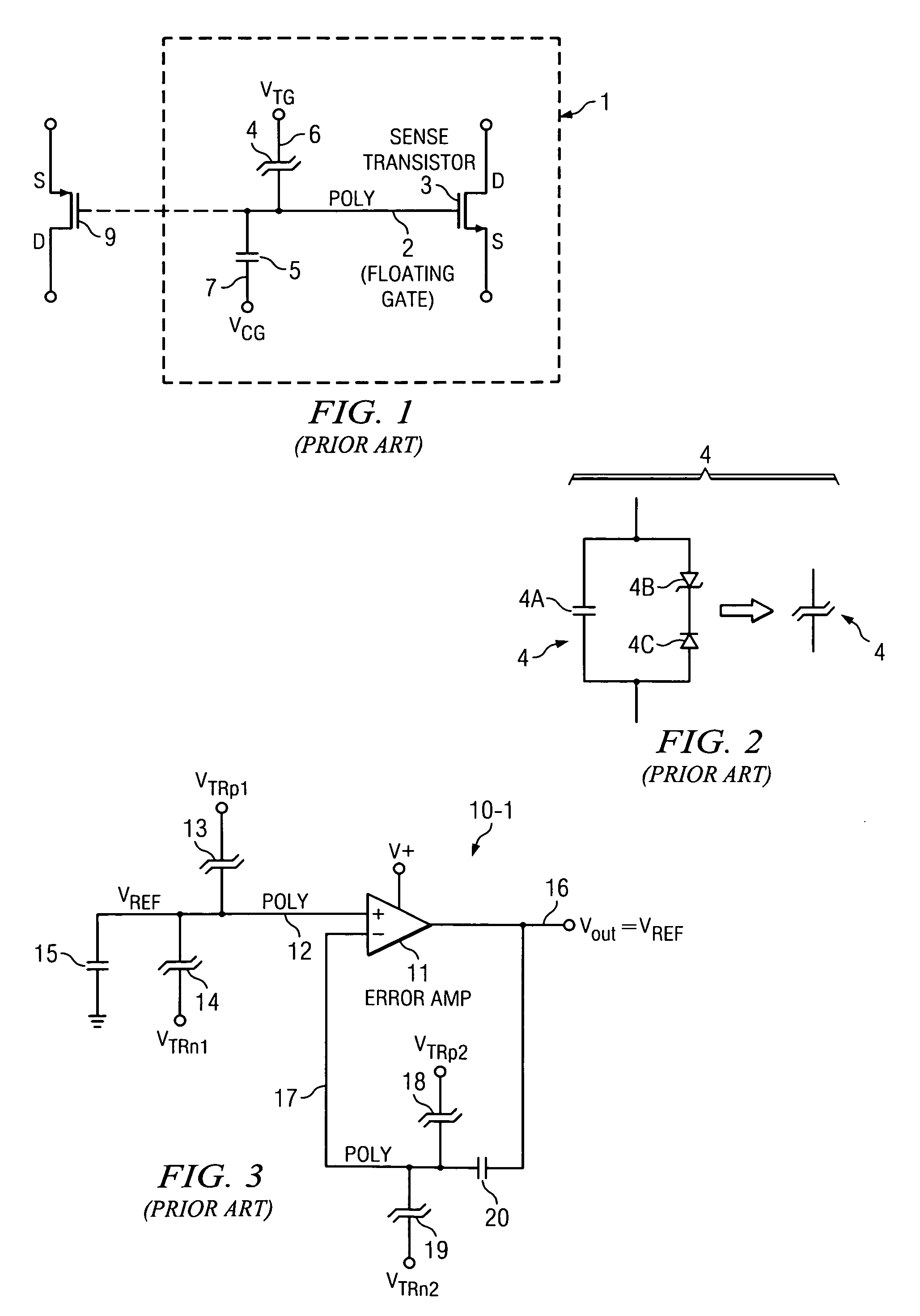
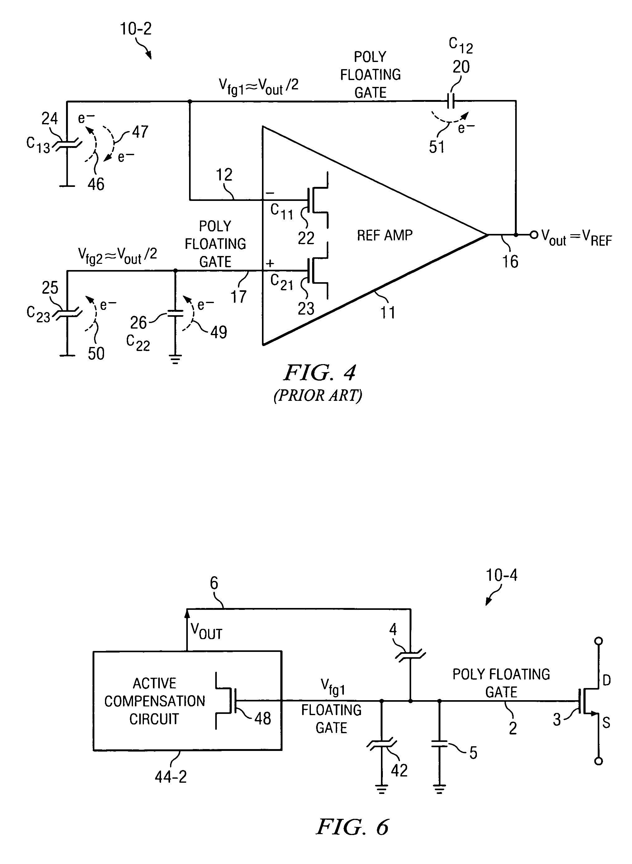
[0067]Referring to FIG. 5, AFG voltage reference circuit 10-3, which may be included in an analog integrated circuit chip, includes error or reference amplifier 11: Reference amplifier 11 has its (−) input connected to the gate of an input transistor 21 in reference amplifier 11 and has its (+) input connected to the gate of an input transistor 23. The gate of (−) input transistor 21 is formed by a portion of floating gate conductor 12. Floating gate 12 also forms a first plate of each of tunneling region 24, tunneling region 31A, tunneling region 31C, and feedback capacitor 20. The capacitances of (−) input transistor 21, (+) input transistor 23, and feedback capacitor 20 are C11, C21, and C12, respectively. The capacitances of tunneling regions 24, 31A, and 31C are C13, C14 and C15, respectively. The second plate of feedback capacitor 20 is connected by conductor 16 to the output of reference amplifier 11, which produces a reference voltage Vout=VREF on conductor 16. The second pl...


PUM


Abstract

An analog floating gate circuit (10-3, 10-4) includes a first sense transistor (21, 3), a first storage capacitor (20, 5), and first (24, 4) and second (31A, 42) tunneling regions. Various portions of a first floating gate conductor (12, 2) form a floating gate of the first sense transistor, a floating first plate of the first storage capacitor (20, 5), a floating first plate of the first tunneling region, and a floating first plate of the second tunneling region, respectively. A second plate of the first storage capacitor is coupled to a first reference voltage (VREF, GND), and a second plate of the second tunneling region is coupled to a second reference voltage (VPROG / GND). Compensation circuitry (44-1, 44-2) is coupled to the first floating gate conductor, for compensating loss of trapped charge from the first floating gate conductor.

Description

BACKGROUND OF THE INVENTION[0001]The present invention relates generally to AFG (analog floating gate) circuits, and more particularly to circuits that compensate for loss of charge stored on analog floating gates used in extremely low power integrated circuits, such as voltage reference circuits.[0002]Floating gate field effect transistors have long been used as digital memory elements. More recently, floating gate field effect transistors have been used in extremely low power analog integrated circuits, such as precision voltage reference circuits.[0003]FIG. 1 shows a conventional EEPROM (electrically erasable programmable read only memory) cell 1 which includes a N-channel floating gate MOS (metal oxide semiconductor) field effect transistor or “sense transistor” or “read transistor”3 having a floating gate electrode 2 disposed on a thin oxide layer over the channel region of the transistor. EEPROM memory is designed to retain a sufficient level of charge on the floating gate MOS...

Claims


Application Information

Patent Timeline
Patent Type & Authority Patents(United States)
IPC IPC(8): G11C27/00
CPCH03F3/45475H03F2203/45546H03F2203/45548
Inventor HELSLEY, DAVID A.MITCHELL, ALLAN T.
Owner TEXAS INSTR INC
Why Eureka
Try Eureka