Memory device and semiconductor device

a memory device and semiconductor technology, applied in information storage, static storage, digital storage, etc., can solve the problems of getting finer, affecting the stability of data storage, so as to achieve the effect of reducing power consumption and reducing power consumption

Active Publication Date: 2014-09-18
SEMICON ENERGY LAB CO LTD
View PDF4 Cites 33 Cited by
  • Summary
  • Abstract
  • Description
  • Claims
  • Application Information

AI Technical Summary

Benefits of technology

[0016]In view of the foregoing problems, an object of one embodiment of the disclosed invention is to provide a memory device that does not need a complicated manufacturing process and has lower power consumption. Another object is to provide a memory device that can have lower power consumption even by stopping the application of power supply voltage for a short time, and specifically a memory device that can have lower power consumption by stopping the application of power supply voltage even when gate leakage is large because of miniaturization of a Si transistor.
[0017]In order to achieve any of the above objects, one embodiment of the present invention uses a memory circuit including a first transistor, a second transistor, and a storage capacitor. One terminal of the storage capacitor is electrically connected to one of a source and a drain of the first transistor and one of a source and a drain of the second transistor. The first and second transistors are transistors with very low off leakage current, for example, transistors using an oxide semiconductor for a channel formation region (OS transistors). Since the off leakage current of the OS transistor is extremely low, a signal held in the storage capacitor can be maintained for a long time. In addition, the memory circuit using the OS transistors as the first and second transistors has the advantage of no performance degradation due to data rewriting.
[0019]The other of the source and the drain of the second transistor may be electrically connected to the second input terminal of the selection circuit through a buffer circuit. If the voltage of the signal held in the storage capacitor is lowered while the application of power supply voltage is stopped, the loss of the voltage can be compensated owing to the buffer circuit at the time of signal output and a proper voltage can be output as a result. When the buffer circuit is provided so that the loss of the voltage can be compensated, the guaranteed operating range of the memory device can be expanded.
[0020]It is possible that the other of the source and the drain of the first transistor is electrically connected to the first input terminal of the selection circuit or the output terminal of the second memory circuit through an inverter circuit, and that the other of the source and the drain of the second transistor is electrically connected to the second input terminal of the selection circuit through another inverter circuit. If the voltage of the signal held in the storage capacitor is lowered while the application of power supply voltage is stopped, the loss of the voltage can be compensated owing to the inverter circuits at the time of signal output and a proper voltage can be output as a result. When the inverter circuits are provided so that the loss of the voltage can be compensated, the guaranteed operating range of the memory device can be expanded.
[0023]According to one embodiment of the disclosed invention, it is possible to provide a lower-power memory device that does not need a complicated manufacturing process. Moreover, it is possible to provide a memory device that can reduce power consumption by stopping the application of power supply voltage even for a short time. Power consumption is effectively reduced particularly when the gate leakage is large because of miniaturization of a Si transistor.

Problems solved by technology

In addition, the structure in FIG. 9 is based on the assumption that the gate leakage current of the Si transistor is sufficiently low; however, design rules for LSI circuits are getting finer and as a result, the gate leakage current of transistors is becoming too high to ignore during the design phase.
Thus, it is becoming difficult to maintain data for a sufficiently long time with the structure in FIG. 9.

Method used


Image

  • Memory device and semiconductor device
  • Memory device and semiconductor device
  • Memory device and semiconductor device

Examples


embodiment 1

Structure of Memory Device in FIG. 1

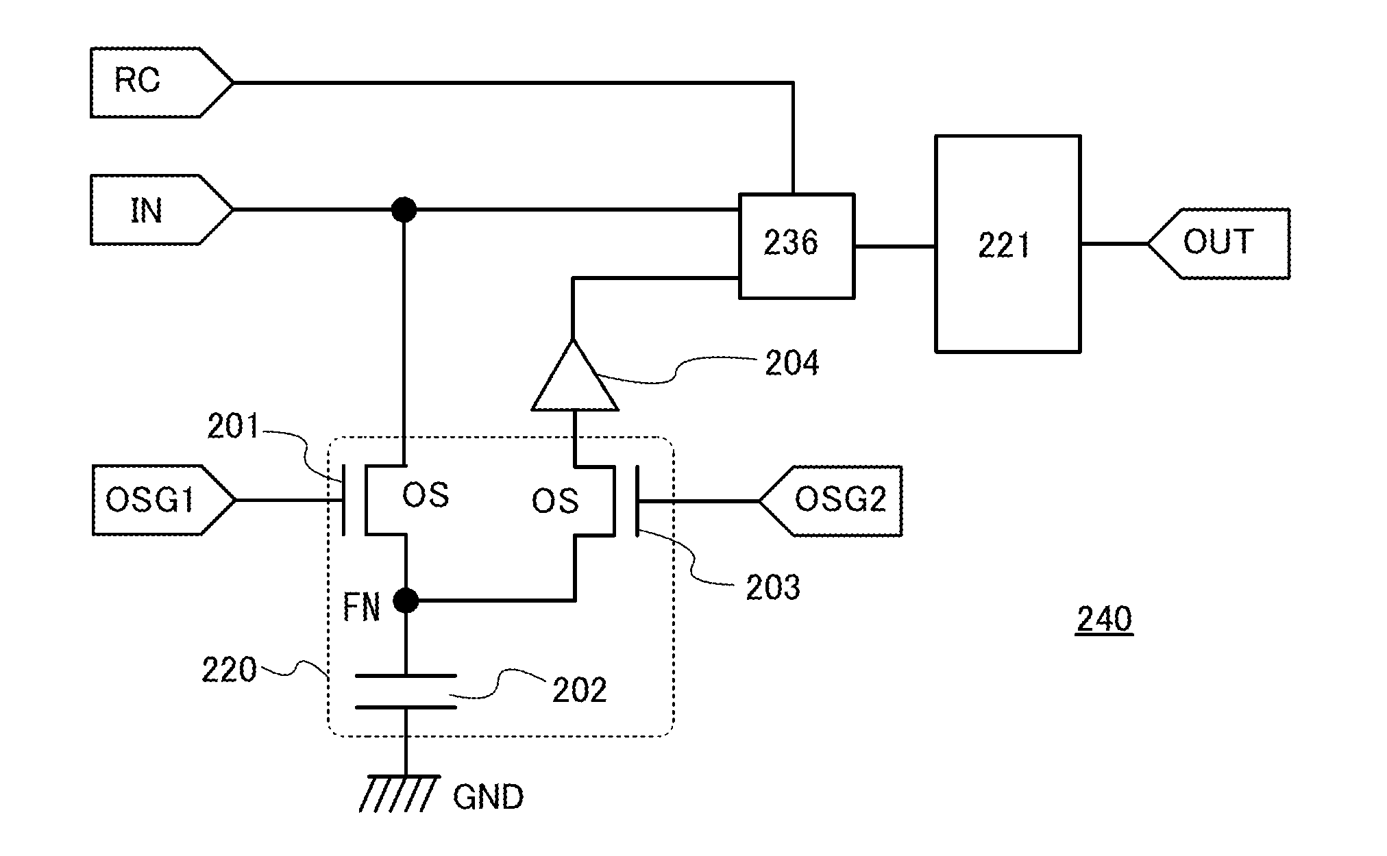
[0039]In Embodiment 1, the structure of a memory device of one embodiment of the present invention will be described with reference to FIG. 1.

[0040]A memory device 240 illustrated in FIG. 1 includes a memory circuit 220 including a first transistor 201, a second transistor 203, and a storage capacitor 202; a memory circuit 221 including a third transistor; and a selection circuit (also referred to as multiplexer) 236 including a fourth transistor.

[0041]As the first transistor 201 and the second transistor 203, a transistor using an oxide semiconductor for a channel formation region (OS transistor) is used, for example. Because of their very low off leakage current, the OS transistors can form the memory circuit 220 in which a signal stored in the storage capacitor 202 can be held during power interruption. The memory circuit 220 including the OS transistors as the first transistor 201 and the second transistor 203 has the advantage of no performan...

embodiment 2

[0064]In Embodiment 2, the structures of a memory device of one embodiment of the present invention that are different from the structure of the memory device in FIG. 1 will be described with reference to FIGS. 3A and 3B.

[0065]FIG. 3A illustrates a structure where a buffer circuit 204 is provided between the other of the source and the drain of the second transistor 203 and the selection circuit 236. The other components are the same as in Embodiment 1. If the voltage of the input signal IN held in the storage capacitor 202 is lowered in the power supply voltage stop period, the loss of the voltage can be compensated owing to the buffer circuit 204 at the time of outputting the signal of the node FN and a proper voltage can be output as a result. When the loss of the voltage can be compensated by providing the buffer circuit 204, the guaranteed operating range of the memory device 240 can be expanded.

[0066]FIG. 3B illustrates a structure where an inverter circuit 205 is provided bet...

embodiment 3

[0068]In Embodiment 3, the structures of a memory device of one embodiment of the present invention that are different from those of the memory devices in FIG. 1 and FIGS. 3A and 3B will be described with reference to FIGS. 4A to 4C and FIGS. 5A to 5c.

[0069]In FIG. 4A, the other of the source and the drain of the first transistor 201 is electrically connected to the output terminal of the memory circuit 221. The other components are the same as in Embodiment 1. Note that the memory circuit 221 in FIG. 4A is configured so that a potential having the same level as the potential of the input signal IN input to the input terminal of the memory circuit 221 is output to the output terminal as the output signal OUT.

[0070]The storage capacitor 202 is connected to the first transistor 201 and the second transistor 203 but not directly connected to the gate of the third transistor or the fourth transistor. Accordingly, even if the gate leakage current of the third transistor or the fourth tr...


PUM


Abstract

A memory device includes a first memory circuit including a silicon transistor, a selection circuit including a silicon transistor, and a second memory circuit including oxide semiconductor transistors and a storage capacitor, in which one terminal of the storage capacitor is connected to a portion where two oxide semiconductor transistors are connected in series, an output of the second memory circuit is connected to a second input terminal of the selection circuit, and an input of the second memory circuit is connected to a first input terminal of the selection circuit or an output terminal of the first memory circuit.

Description

BACKGROUND OF THE INVENTION[0001]1. Field of the Invention[0002]The present invention relates to an object, a method, or a manufacturing method. Further, the present invention relates to a process, a machine, manufacture, or a composition of matter. For example, in this specification, a semiconductor device, a display device, a power storage device, driving methods thereof, and manufacturing methods thereof are described. In this specification, as the semiconductor device, for example, a memory circuit, a processor including a memory circuit (typically, a programmable logic device, a CPU, or a microcontroller), and an electronic device including the processor are described.[0003]Note that in this specification, a semiconductor device means a device including a circuit having a semiconductor element (e.g., a transistor or a diode). Alternatively, the semiconductor device means any device that can function by utilizing semiconductor characteristics. For example, an integrated circuit,...

Claims


Application Information

Patent Timeline
Patent Type & Authority Applications(United States)
IPC IPC(8): G11C11/24
CPCG11C11/24G11C11/403Y02D10/00G11C11/401G11C11/4093
Inventor TSUTSUI, NAOAKIISOBE, ATSUOUESUGI, WATARUOHMARU, TAKURO
Owner SEMICON ENERGY LAB CO LTD
Why Eureka
Try Eureka