Semiconductor laser device, optical transmission device, optical transmission system, electronic device, control device, connector, communication device, and optical transmission method and data transmission and reception method

a laser device and semiconductor technology, applied in the direction of semiconductor lasers, electromagnetic transceivers, laser structures, etc., can solve the problems of difficult to obtain a modulated frequency higher than about 50 mhz, impossible high-speed modulation, and huge power consumption in long-range transmission, so as to achieve the effect of avoiding connection collision, simplifying communication protocols, and high-speed modulation

Inactive Publication Date: 2005-07-28
SHARP KK
View PDF34 Cites 11 Cited by
  • Summary
  • Abstract
  • Description
  • Claims
  • Application Information

AI Technical Summary

Benefits of technology

[0069] In the present invention, the semiconductor laser chip and the molded resin having a light diffusion capability are combined so that a light beam emitted from the semiconductor laser chip is safely released into a space after being diffused by the molded resin, thereby making it possible to achieve high-speed transmission with low power consumption as compared with LEDs.
[0082] Thus, the invention described herein makes possible the advantages of (1) providing a semiconductor laser device, an optical transmission device, an electronic device and a space optical transmission system, and a control device and a communication device thereof, and a space optical transmission method and a data transmission and reception method, which realize high-speed modulation, low power consumption, the safety of eyes, and high reliability, and which are suitable for the space optical transmission and realize full-duplex space optical transmission; and (2) providing a semiconductor laser device, an optical transmission device, an electronic device and a fiber optical transmission system, and a control device and a communication device thereof, and a fiber optical transmission method and a data transmission and reception method, which realize high-speed transmission, low power consumption, and easy alignment with a fiber, and which are suitable for the fiber optical transmission and realize full-duplex fiber optical transmission.

Problems solved by technology

Now commercially available LEDs are not suitable for higher speed and longer distance transmission in view of the following two points: (1) high-speed modulation is impossible due to the limitations of high-speed response characteristics of the LED; and (2) power consumption is enormous in long distance transmission.
It is difficult to obtain a modulated frequency higher than about 50 MHz.
Moreover, special LEDs capable of high-speed modulation dissipate very high power.
However, the semiconductor laser light beam itself exceeds a safety level of eyes, so that it is not allowable to emit the semiconductor laser light beam directly into a space.
Moreover, the reliability of the semiconductor laser devices may be deteriorated during the high-output operation.
Furthermore, the space optical transmission system is not capable of full-duplex transmission.
This is a serious problem.
Accordingly, when two-way communication is tested using two transmission and reception units, full-duplex communication cannot be attained.
It is not as easy as the alignment of the LED and the POF.
It is not possible to establish the full-duplex communication using a single fiber.

Method used


Image

  • Semiconductor laser device, optical transmission device, optical transmission system, electronic device, control device, connector, communication device, and optical transmission method and data transmission and reception method
  • Semiconductor laser device, optical transmission device, optical transmission system, electronic device, control device, connector, communication device, and optical transmission method and data transmission and reception method
  • Semiconductor laser device, optical transmission device, optical transmission system, electronic device, control device, connector, communication device, and optical transmission method and data transmission and reception method

Examples


embodiment 1

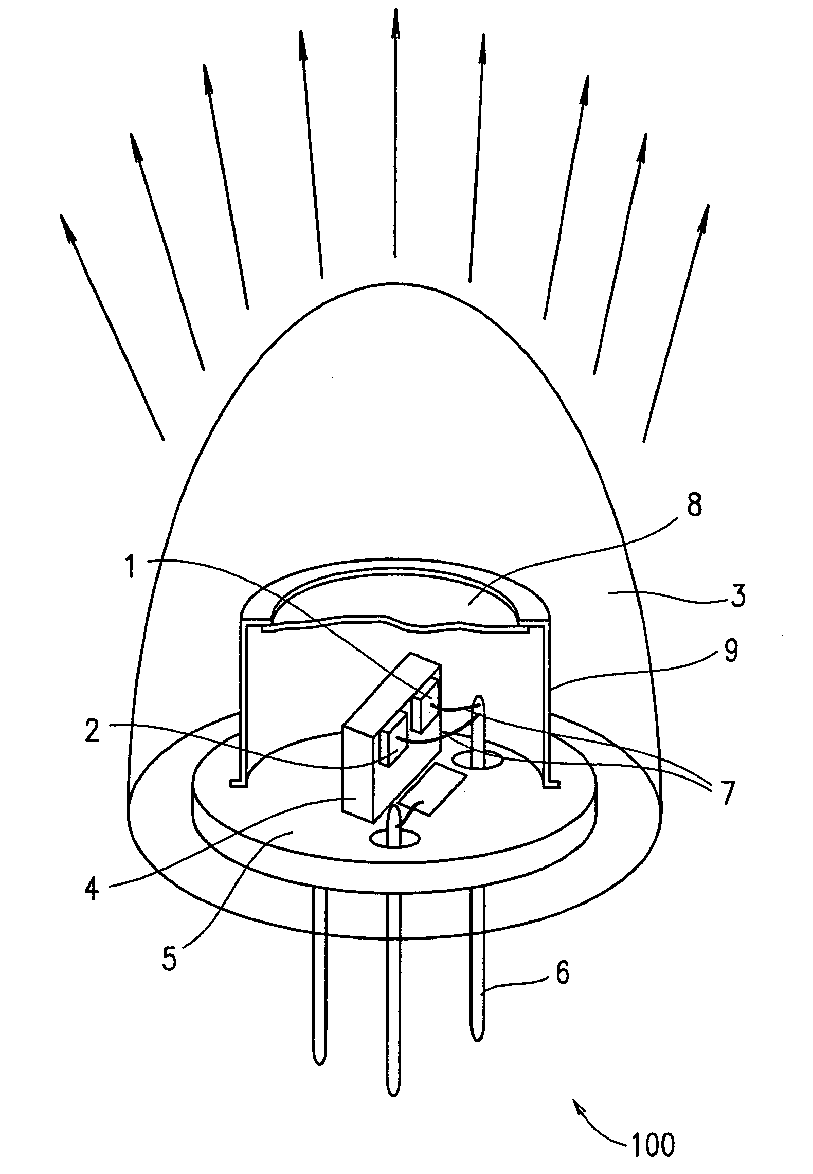
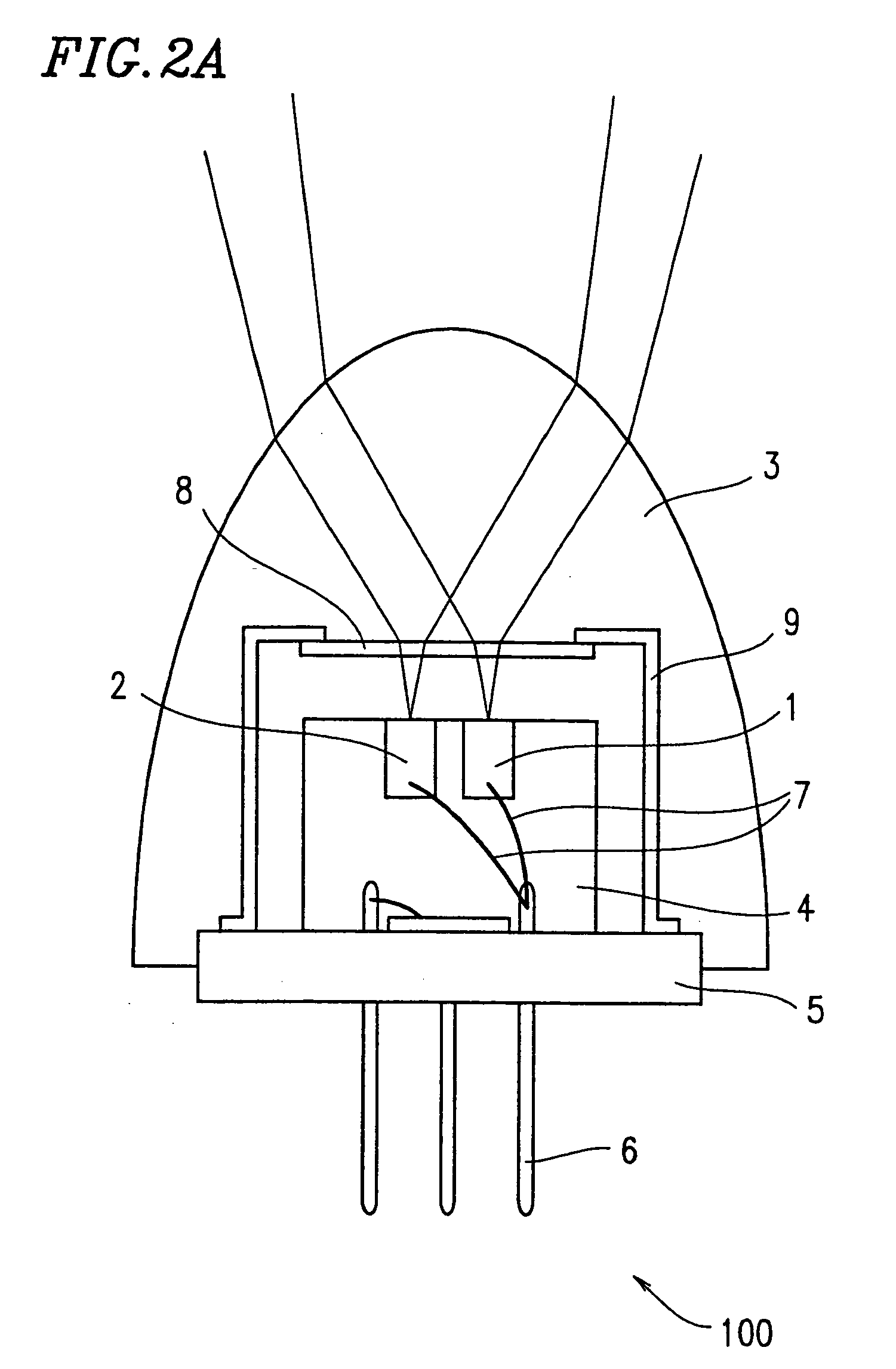
[0106]FIG. 1 is a perspective view showing a semiconductor laser device 100 according to Embodiment 1 of the present invention. FIG. 2A is a cross-sectional view thereof. The semiconductor laser device 100 includes two semiconductor laser chips 1 and 2 which are contained in a typical semiconductor laser package. The package are entirely covered with a molded resin 3. The semiconductor laser chips 1 and 2 are fixed to a heat sink 4 which is integrally molded with a metal stem 5. The semiconductor laser chips 1 and 2 have a satisfactory heat radiation capability. In Embodiment 1, the thermal resistance of each of the packages of the semiconductor laser chips 1 and 2 is about 90 deg / W. Surfaces opposite to the heat sink 4 of the semiconductor laser chips 1 and 2 are electrically connected to each other via a common lead-pin 6 and a wire 7. Accordingly, the semiconductor laser chips 1 and 2 are connected to each other in parallel, so that a current is simultaneously supplied to the sem...

embodiment 2

[0126]FIG. 3 is a cross-sectional view showing a semiconductor laser device 300 according to Embodiment 2 of the present invention. In Embodiment 2, the semiconductor laser device 300 includes a multi-stripe semiconductor laser chip 11 (so-called semiconductor laser array). In FIG. 3, the stripe of a light emitting portion of the multi-stripe semiconductor laser chip 11 is not shown, but a pattern of the emitted light beams is shown.

[0127] In the semiconductor laser device 300, the multi-stripe semiconductor laser chip has a plurality of light emitting portions (stripes), so that the resistance of the semiconductor laser chip is decreased. Therefore, a driving voltage can be reduced. Further, similar to Embodiment 1, the spot size of the emitted light beam can be increased by adjusting the distance between the light emitting portions while maintaining the radiation angle. The light density at a light emitting facet of the semiconductor laser chip can be reduced, thereby securing th...

embodiment 3

[0132]FIG. 4 is a perspective view showing a semiconductor laser device 400 according to Embodiment 3 of the present invention. In Embodiment 3, the semiconductor laser device 400 includes a semiconductor laser package including two semiconductor laser chips 12 and 13. The semiconductor laser device 400 differs from that of Embodiment 1 in the following points.

[0133] 1. The semiconductor laser chips 12 and 13 have different oscillation wavelengths. In Embodiment 3, the semiconductor laser chip 12 has an oscillation wavelength of about 980 nm. The semiconductor laser chip 13 has an oscillation wavelength of about 920 nm.

[0134] 2. The semiconductor laser chips 12 and 13 are connected via the respective wires to different lead-pins 6 and 66, respectively. Accordingly, the package includes one more lead-pin than Embodiment 1.

[0135] Next, a transmission and reception unit 500 including the semiconductor laser device 400, and a space optical transmission system using the transmission a...


PUM


Abstract

A device including a semiconductor laser device having a semiconductor laser chip, and a molded resin having a light diffusion capability. The semiconductor laser chip is covered with the molded resin.

Description

BACKGROUND OF THE INVENTION 1. Field of the Invention [0001] The present invention relates to a semiconductor laser device which is used in applications, such as a light source for wireless communication and sensing, where the device emits a light beam into a space and a human may see the light beam directly from its light source, and which ensures the safety of eyes. The present invention also relates to an optical transmission device and an optical transmission system using the above-described semiconductor laser device. The present invention still further relates to an electronic device, a control device, and a communication device using the above-described optical transmission device or optical transmission system, such as a personal computer, a personal digital assistant, or a digital camera. The present invention further relates to a space optical transmission method and a data transmission and reception method. Moreover, the present invention is directed to a semiconductor la...

Claims


Application Information

Patent Timeline
Patent Type & Authority Applications(United States)
IPC IPC(8): H01L31/0232H01S3/04H01S5/00H01S5/02H01S5/022H01S5/024H01S5/40H04B10/079H04B10/11H04B10/40H04B10/50H04B10/60
CPCH01L33/58H01S5/005H01S5/02212H01S5/0222H01S5/02228H01S5/4087H01S5/02284H01S5/02288H01S5/024H01S5/4025H01S5/02232H01L2224/48091H01L2224/48247H01L2224/49113H01S5/02234H01S5/02253H01S5/02251H01L2924/00014
Inventor KAWANISHI, HIDENORIINOOKA, TOSHIHIROSHIMONAKA, ATSUSHIKUMATANI, KEIJI
Owner SHARP KK
Why Eureka
Try Eureka