

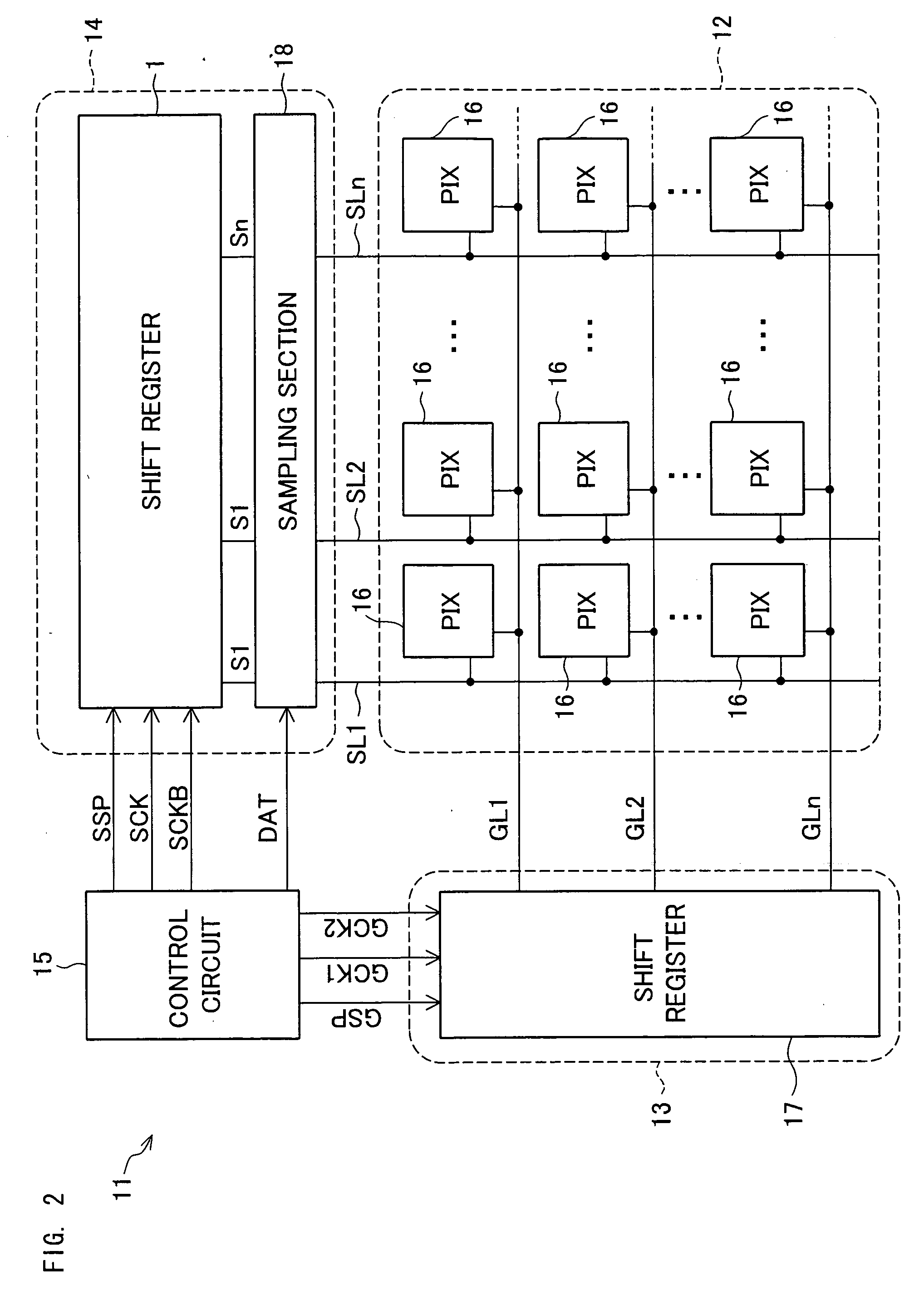
Flip-flops, shift registers, and active-matrix display devices
a shift register and display device technology, applied in pulse generators, pulse techniques, instruments, etc., can solve problems such as signal delay, desired data may not be properly sent to the source line, and the output signal may not be sent out properly, so as to reduce the signal delay and improve the rise and fall characteristics
- Summary
- Abstract
- Description
- Claims
- Application Information
AI Technical Summary
Benefits of technology
Problems solved by technology
Method used
Image

Examples
first embodiment
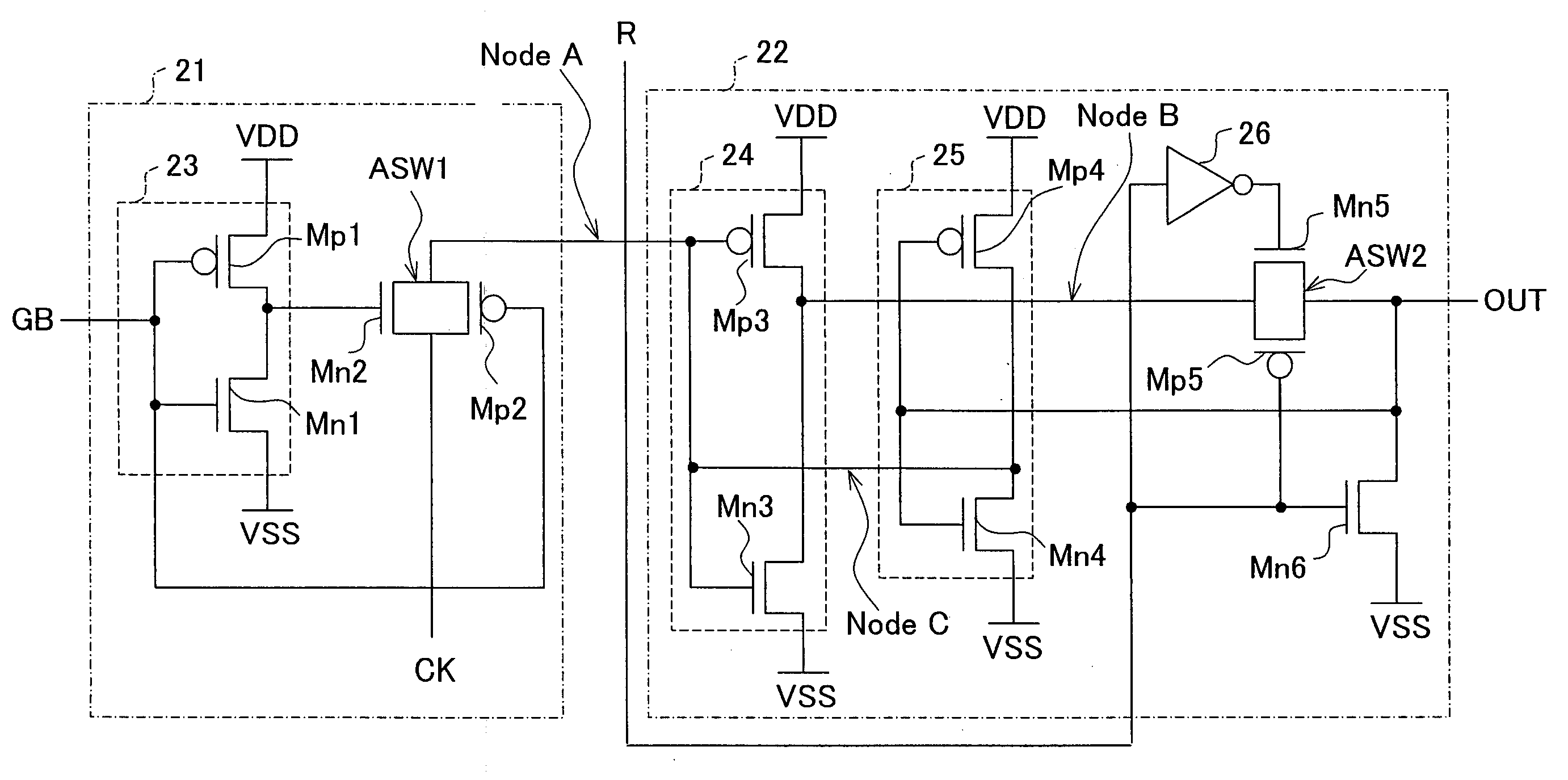
[0106] Referring to FIG. 1, the following will describe an exemplary structure of an RS flip-flop according to the First Embodiment.
[0107] The RS flip-flop shown in FIG. 1 has two major parts, a gating section 21 and a latch section 22.
[0108] The gating section 21 includes an inverter circuit 23 realized with a p-type transistor Mp1 and an n-type transistor Mn1 (hereinafter, p-type transistors and n-type transistors will be denoted by Mp and Mn, respectively), which are connected in series between power supply VDD (high potential) and VSS (low potential). A control terminal GB is connected to the input side of the inverter circuit 23, i.e., to the gates of the Mp1 and Mn1.
[0109] Between an input terminal CK and Node A is connected a CMOS analog switch ASW1 connecting Mn2 and Mp2 in parallel. In the analog switch ASW1, the gate of the Mn2 is connected to the output of the inverter circuit 23 (i.e., the junction connecting the source of Mp1 and the drain of Mn1), and the gate of Mp...
second embodiment
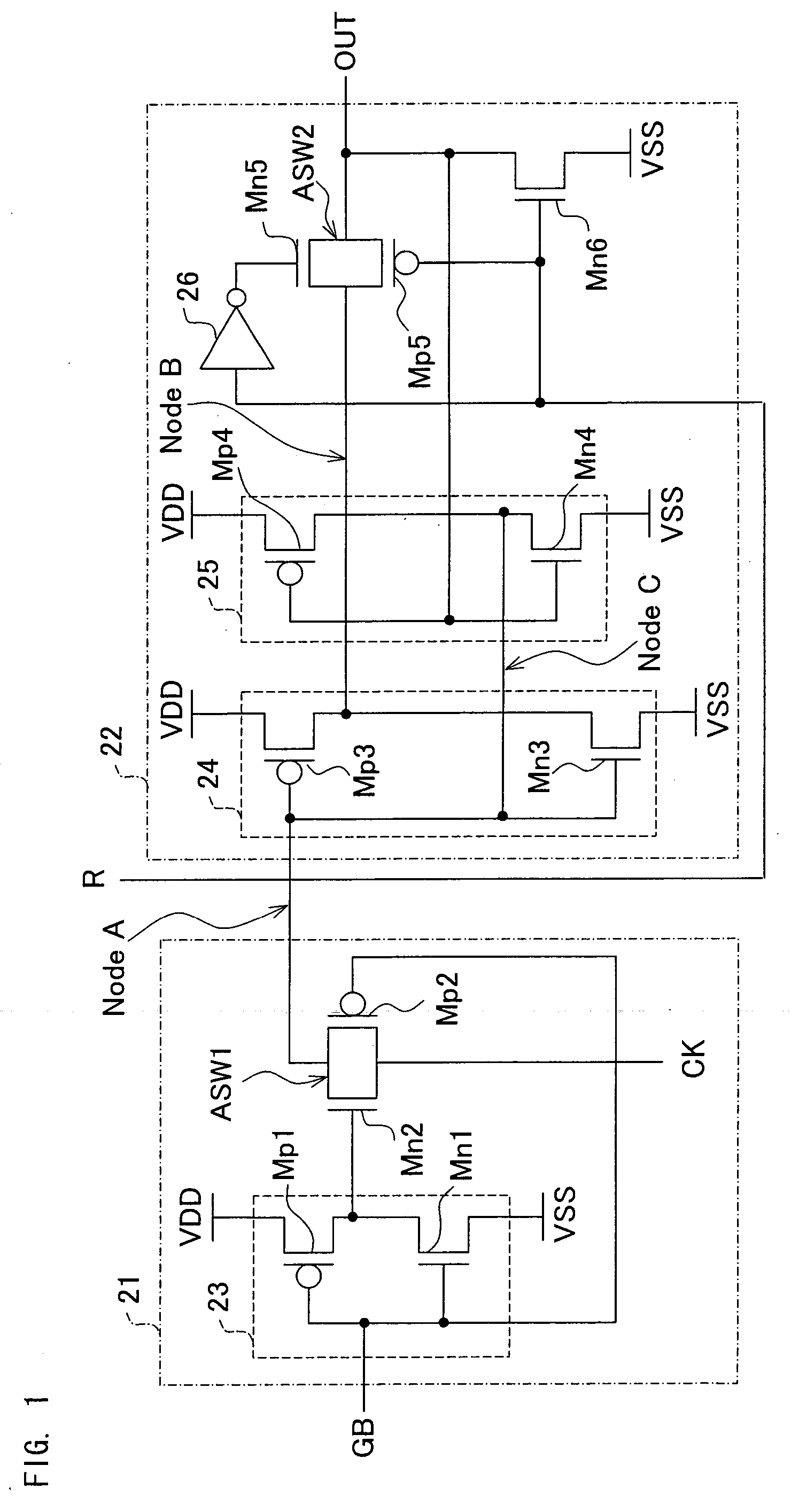
[0136] Referring to FIG. 5, the following will describe an exemplary structure of an RS flip-flop according to another embodiment of the invention.
[0137] The RS flip-flop shown in FIG. 5 includes two major parts, a gating section 21 and a latch section 27. As to a structure and operations of the gating section 21, no further explanation will be made because they are essentially the same as those in the RS flip-flop of the First Embodiment described with reference to FIG. 1.
[0138] The latch section 27 is similar to the latch 22 but includes an analog switch ASW3 instead of the analog switch ASW2. It is to be noted that elements of the latch section 27 having similar structures as those of the latch section 22 are given the same reference symbols and further explanations thereof will be omitted.
[0139] The analog switch ASW3 is connected between the output of the inverter 24 and the output terminal OUT of the RS flip-flop, and it serves as a CMOS analog switch connecting Mn7 and Mp7...
third embodiment
[0155] Referring to FIG. 7, the following will describe an exemplary structure of an RS flip-flop according to yet another embodiment of the invention.
[0156] The RS flip-flop shown in FIG. 7 includes two major parts, a gating section 28 and a latch section 22. As to a structure and operations of the latch section 22, no further explanation will be made because they are essentially the same as those in the RS flip-flop of the First Embodiment described with reference to FIG. 1.
[0157] The gating section 28 is structured such that it receives a control signal GB, a clock signal CK, and an inverted clock signal CKB, wherein the clock signal CK and inverted clock signal CKB have amplitudes smaller than that produced by VDD, which is a power supply of the flip-flop.
[0158] In the gating section 28, Mp8 and Mn8 are connected in series between the power supply VDD and the input terminal CKB, and an Mn9 is connected between the input terminal CK and the Node A (output of the gating section...
PUM
 Abstract
Description
Claims
Application Information