
Differential voltage control oscillator including radio-frequency switching circuits
- Summary
- Abstract
- Description
- Claims
- Application Information
AI Technical Summary
Benefits of technology
Problems solved by technology
Method used
Image



Examples
first embodiment
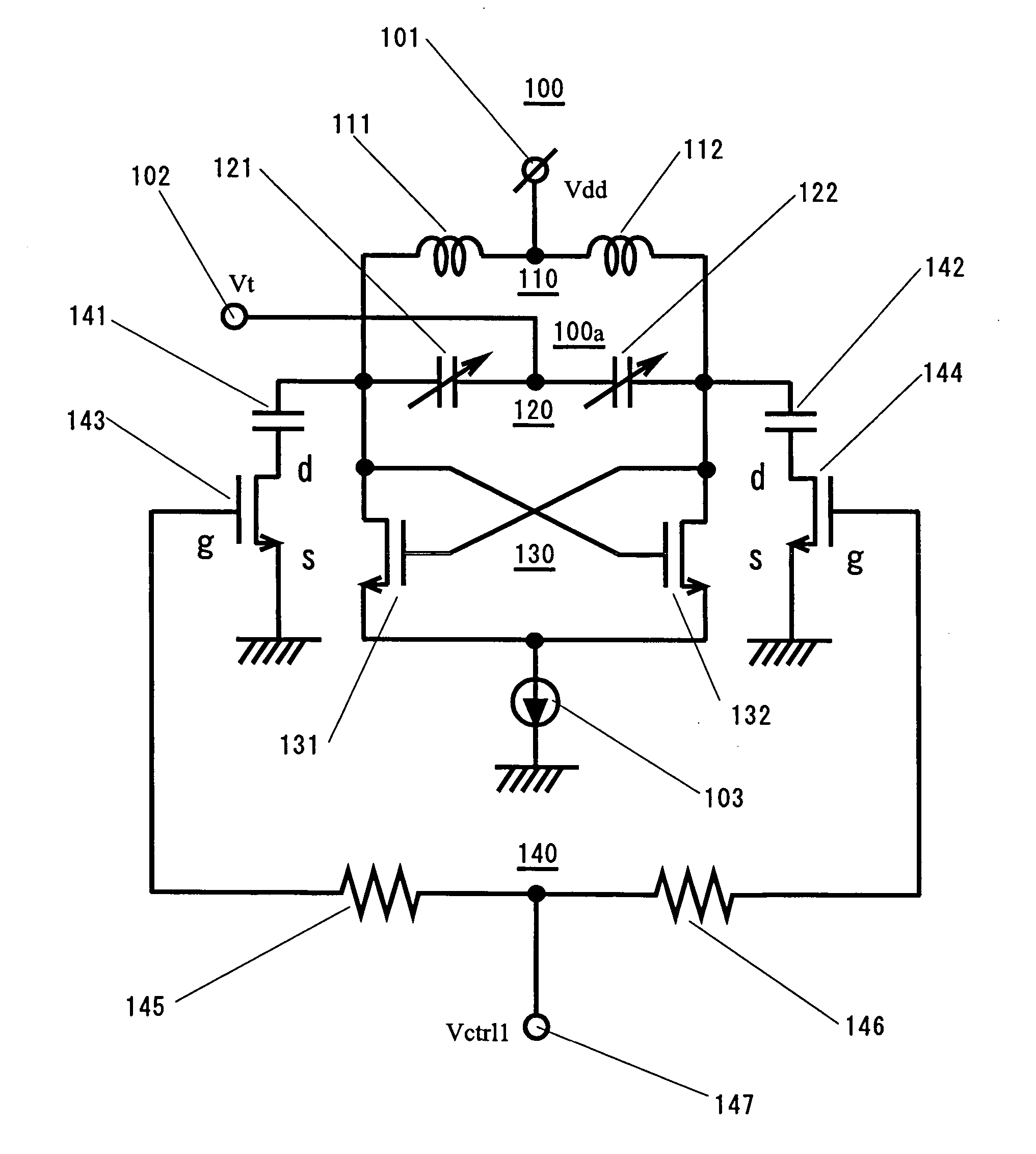
[0128]FIG. 1 is a circuit diagram illustrating a differential voltage control oscillator 100 including a radio-frequency switching circuit 140 according to a first embodiment of the present invention. Note that the differential voltage control oscillator 100 is suitable for use in a frequency band between 800 MHz and 5 GHz where mobile telephones operate under the global system for mobile communications (GSM) technology or the personal digital cellular (PDC) technology.
[0129] The differential voltage control oscillator 100 shown in FIG. 1 includes a parallel resonance circuit 100a and a negative resistance circuit 130.
[0130] The parallel resonance circuit 100a includes an inductor circuit 110, a variable capacitance circuit 120, and a radio-frequency switching circuit 140. In the differential voltage control oscillator 100, the inductor circuit 110, the variable capacitance circuit 120, the negative resistance circuit 130, and the radio-frequency switching circuit 140 are connecte...
second embodiment
[0209]FIG. 11 is a circuit diagram illustrating a radio-frequency switching circuit 240 according to a second embodiment of the present invention. In FIG. 11, elements similar to those of the radio-frequency switching circuit 140 according to the first embodiment are denoted by the same reference numerals, and the descriptions thereof are omitted.
[0210] The radio-frequency switching circuit 240 according to the second embodiment is the same as the radio-frequency switching circuit 140 according to the first embodiment, except that a resistive element 241 is disposed between a connection point of the resistive elements 145 and 146 and a control voltage terminal 147. That is, the radio-frequency switching circuit 240 according to the second embodiment has an impedance element interposed between a virtual ground point and the control voltage terminal 147.
[0211] In the radio-frequency switching circuit 240, the resistive elements 145, 146, and 241 act as radio-frequency signal reducti...
third embodiment
[0213]FIG. 12 is a circuit diagram illustrating a radio-frequency switching circuit 340 according to a third embodiment of the present invention. In FIG. 12, elements similar to those of the radio-frequency switching circuit 140 according to the first embodiment are denoted by the same reference numerals, and the descriptions thereof are omitted.
[0214] The radio-frequency switching circuit 340 according to the third embodiment is the same as the radio-frequency switching circuit 140 according to the first embodiment, except that there is no element corresponding to the resistive element 146, and a resistive element 241 is disposed between a control voltage terminal 147 and a connection point of a resistive element 145 and a switching element 144.
[0215] In the radio-frequency switching circuit 340, the resistive elements 145 and 241 act as radio-frequency signal reduction sections associated with a switching element 143. Further, the resistive element 241 acts as a fourth radio-fre...
PUM
 Abstract
Description
Claims
Application Information