Applications of Raman scattering probes

a raman scattering and probe technology, applied in the field of application of raman scattering probes, can solve the problems of neglected and overlooked wide range of applications that should be achievable with relative low raman sensitivity detections implementing conventional raman scattering

Inactive Publication Date: 2005-09-22
OPTOTRACE TECH
View PDF7 Cites 66 Cited by
  • Summary
  • Abstract
  • Description
  • Claims
  • Application Information

AI Technical Summary

Benefits of technology

[0014] Furthermore, a wide range of applications that should be achievable with relative low Raman sensitivity detections implementing conventional Raman Scattering were also overlooked and neglected due to low expectation of Raman sensing capabilities. New and improved Raman sensing applications are also disclosed in this invention that do not require high detection sensitivities and do not require surface enhanced Raman sensing devices such as such RamanNanoChip™ applications. The embodiments disclosed in this invention thus expand the fields of applications for devices that implement Raman scattering sensing technologies.

Problems solved by technology

Furthermore, a wide range of applications that should be achievable with relative low Raman sensitivity detections implementing conventional Raman Scattering were also overlooked and neglected due to low expectation of Raman sensing capabilities.

Method used


Image

  • Applications of Raman scattering probes
  • Applications of Raman scattering probes
  • Applications of Raman scattering probes

Examples


Embodiment Construction

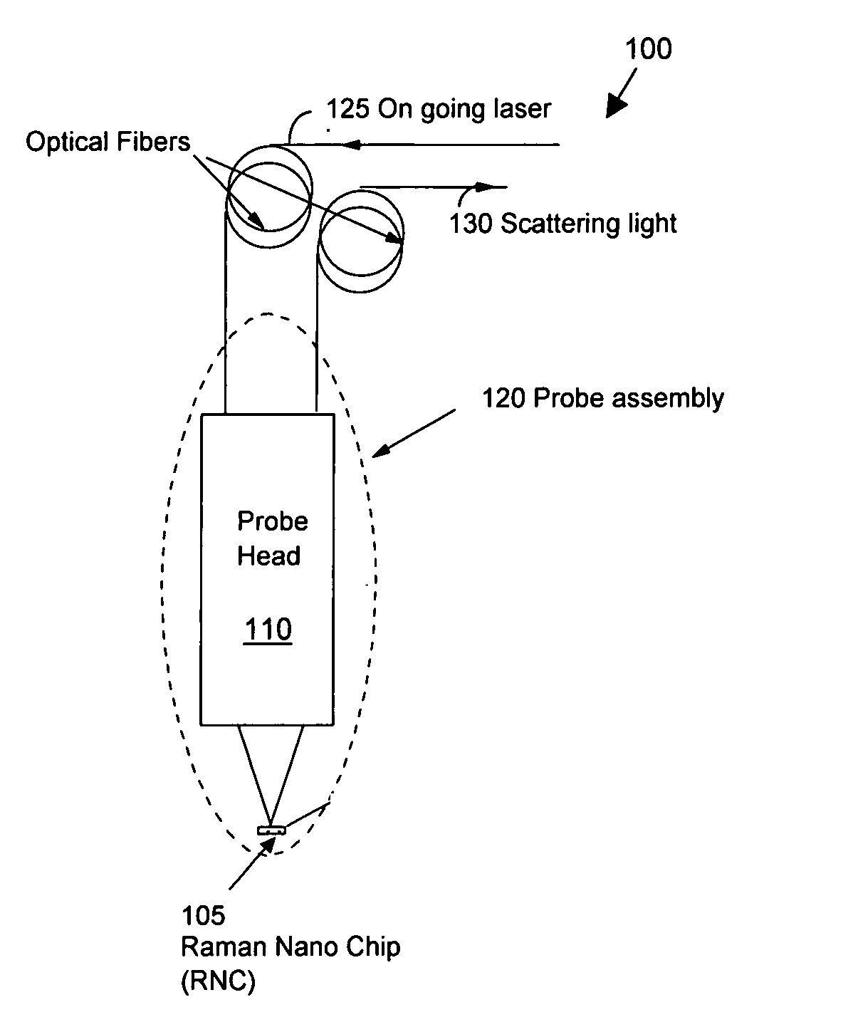
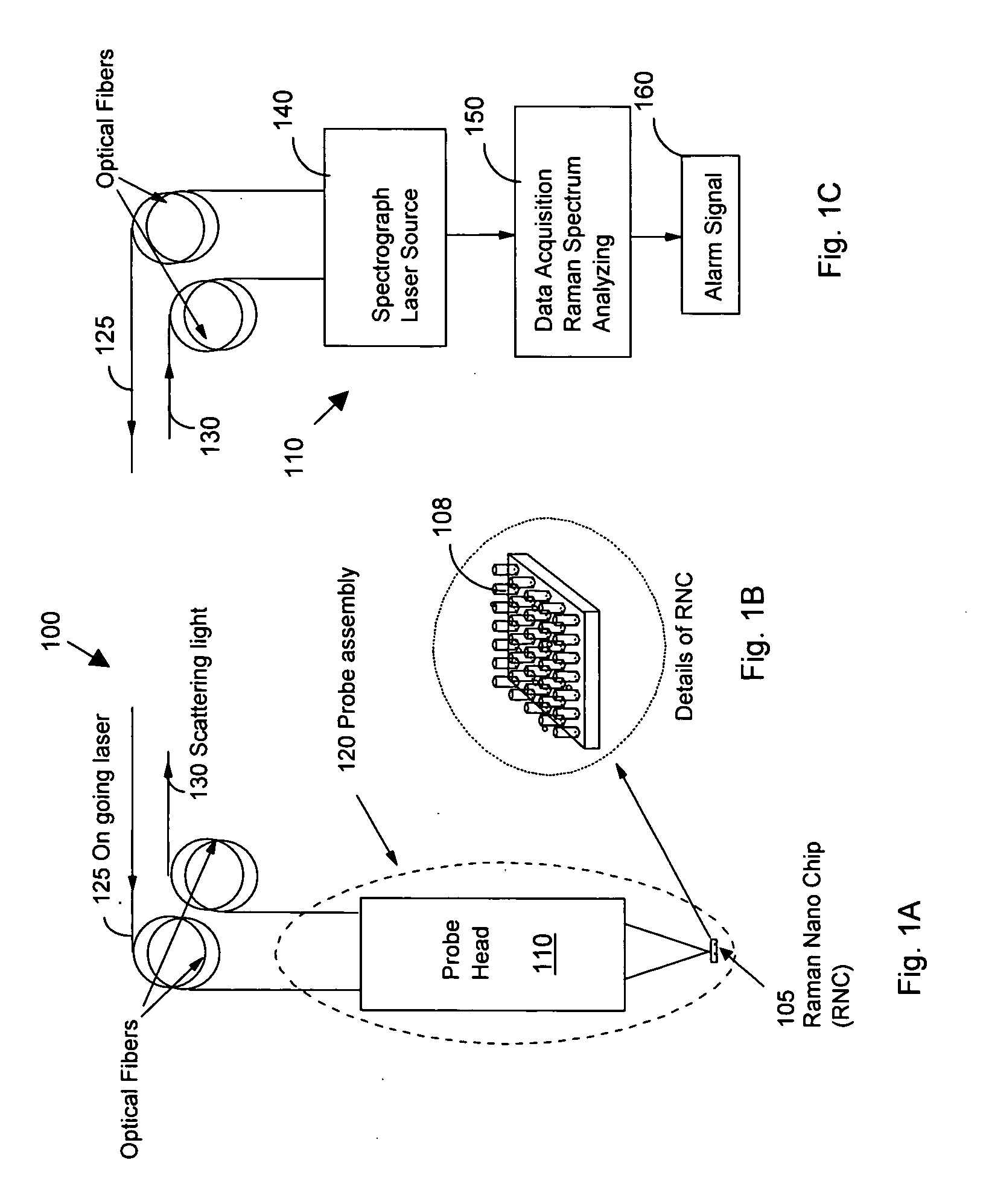
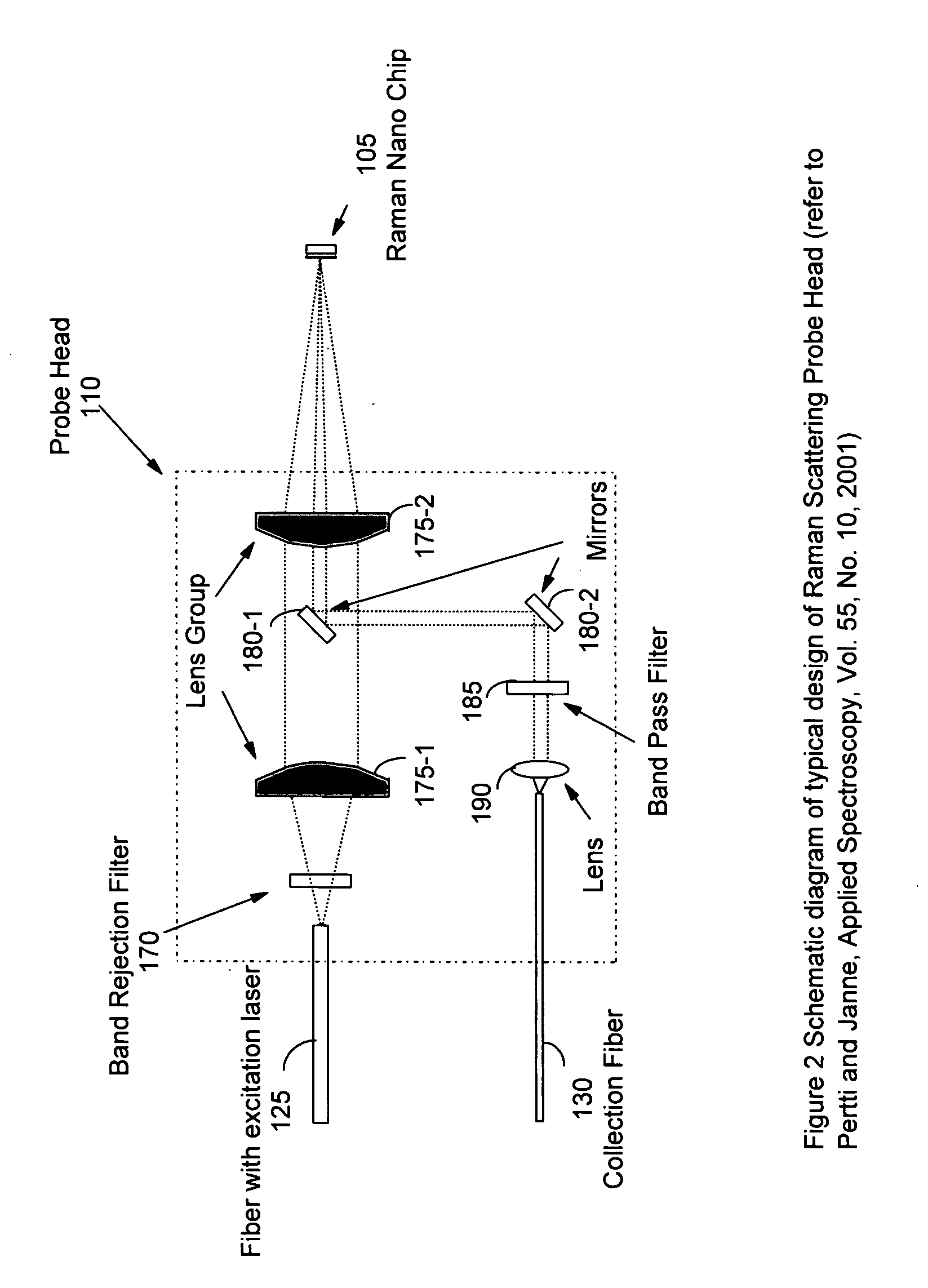
[0027] Refer to FIG. 1A for a basic configuration of a Raman detector 100 using a RamanNanoChip™105 attached to a probe head 110. As shown in FIG. 1B, a RamanNanoChip™105 includes a plurality of nano-sticks 108 as that disclosed in the co-pending application Ser. No. 10 / 852,287 filed on May 24, 2004 and implemented in this patent application as an expanded Surface Enhance Raman Sensing System. The probe head 110 with a RamanNanoChip™105 is placed in a space under monitoring. The probe assembly as shown may includes design features such as a vacuum pump to suck air flow into a probe assembly 120 enclosed in a housing structure shown with dotted lines to trap molecules of gas, liquid, and solid powder for carrying out a Raman scattering detection operation. An excitation laser is led by optical fibers 125 from frame of the Raman Spectroscope and laser source 140 shown in FIG. 1C that can be placed in central office far away from the monitoring field. The probe head 110 is pre-aligned ...


PUM

PropertyMeasurementUnit
optical scatteringaaaaaaaaaa
chemical compositionaaaaaaaaaa
Raman scatteringaaaaaaaaaa

Abstract

New and improved applications of Raman Scattering are disclosed. These applications may be implemented with or without using an enhanced nano-structured surface that is trademarked as the RamanNanoChip™ disclosed in a pending patent. As a RamanNanoChip™ provides much higher sensitivity in SERS compared with conventional enhance surface, broader scopes of applications are now enabled and can be practically implemented as now disclosed in this application. Furthermore, a wide range of applications is achievable as new and improved Raman sensing applications. By applying the analysis of Raman scattering spectrum, applications can be carried out to identify unknown chemical compositions to perform the tasks of homeland security; food, drug and drinking materials safety; early disease diagnosis; environmental monitoring; industrial process monitoring, precious metal and gem authentications, etc.

Description

[0001] This application is a Continuation in Part (CIP) application of another co-pending application Ser. No. 10 / 852,287 filed on May 24, 2004. application Ser. No. 10 / 852,287 claims a Priority Date of May 27, 2003, benefited from two previously filed Provisional Applications 60 / 473,283 and 60 / 473,287 filed on May 27, 2003, and another Provisional Application 60 / 520,222 filed on Nov. 17, 2003 by at least one of a common Applicant of this patent application.BACKGROUND OF THE INVENTION [0002] 1. Field of the Invention [0003] This invention relates generally to the methods and systems for detection of very small amount of trace chemicals by employing light scattering probes. More particularly, this invention relates to an improved light scattering probes and detection system implemented with highly sensitive Raman analyzer embodied as RamanNanoChip™ based on a novel process to fabricate a sensing chip with nano-structured noble metal surface with improved configurations to detect the ...

Claims


Application Information

Patent Timeline
Patent Type & Authority Applications(United States)
IPC IPC(8): G01J3/44G01N21/65
CPCG01J3/44G08B21/12G01N21/658
Inventor WANG, HONGLIU, ZHIMIN
Owner OPTOTRACE TECH
Why Eureka
Try Eureka