Lithographic apparatus, device manufacturing method

a technology of lithographic apparatus and manufacturing method, which is applied in the direction of optical elements, photomechanical devices, instruments, etc., can solve the problems of destroying or affecting the state polarization of radiation traversing the optical elements downstream of the illumination system, depolarization or a change of polarization affecting image contrast beyond tolerance, and achieves the effect of improving control over the state of radiation polarization

Inactive Publication Date: 2006-04-13
ASML NETHERLANDS BV
View PDF2 Cites 85 Cited by
  • Summary
  • Abstract
  • Description
  • Claims
  • Application Information

AI Technical Summary

Problems solved by technology

However, optical elements downstream of the illumination system may destroy or affect the state polarization of radiation traversing these elements due to, for example, the presence of residual or inherent optical birefringence in the material of the elements or due to effects of optical (single or multi-layer) coatings on the element surfaces.
However, optical elements not being a fixed part of the optical system, such as for example a patterning device embodied as a reticle, may cause a depolarization or a change of polarization affecting image contrast beyond tolerance.

Method used


Image

  • Lithographic apparatus, device manufacturing method
  • Lithographic apparatus, device manufacturing method
  • Lithographic apparatus, device manufacturing method

Examples


Embodiment Construction

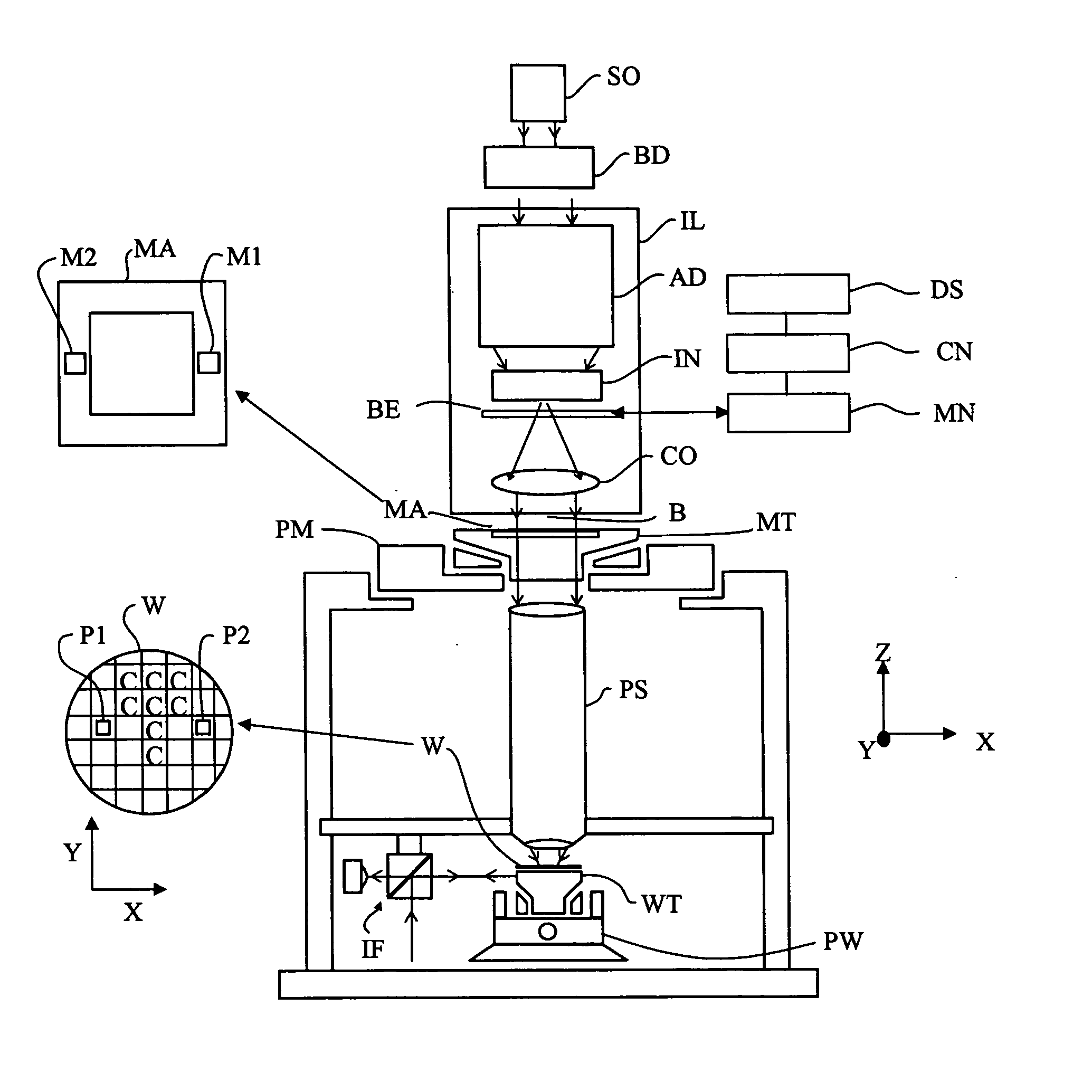
[0025]FIG. 1 schematically depicts a lithographic apparatus according to one embodiment of the invention. The apparatus comprises:

[0026] an illumination system (illuminator) IL configured to condition a radiation beam B (e.g., UV radiation such as for example generated by an excimer laser operating at a wavelength of 193 nm or 157 nm radiation);

[0027] a support structure (e.g., a mask table) MT constructed to support a patterning device (e.g., a mask) MA and connected to a first positioner PM configured to accurately position the patterning device in accordance with certain parameters;

[0028] a substrate table (e.g., a wafer table) WT constructed to hold a substrate (e.g., a resist-coated wafer) W and connected to a second positioner PW configured to accurately position the substrate in accordance with certain parameters;

[0029] a projection system (e.g., a refractive projection lens system) PS configured to project a pattern imparted to the radiation beam B by patterning device M...


PUM


Abstract

To compensate for birefringence of a mask in a lithographic projection apparatus, the birefringence of a mask is measured and stored as birefringence data in a data storage device. A birefringent compensation element is disposed in the optical path of the lithographic projection apparatus. Appropriate adjustments of the compensation element are determined as those optimally reducing impact of the mask birefringence on the state of polarization at substrate level.

Description

BACKGROUND OF THE INVENTION [0001] 1. Field of the Invention [0002] The present invention relates to a lithographic apparatus, and a device manufacturing method. [0003] 2. Description of the Related Art [0004] A lithographic apparatus is a machine that applies a desired pattern onto a substrate, usually onto a target portion of the substrate. A lithographic apparatus can be used, for example, in the manufacture of integrated circuits (ICs). In that instance, a patterning device, which is alternatively referred to as a mask or a reticle, may be used to generate a circuit pattern to be formed on an individual layer of the IC. This pattern can be transferred onto a target portion (e.g., comprising part of, one, or several dies) on a substrate (e.g., a silicon wafer). Transfer of the pattern is typically via imaging onto a layer of radiation-sensitive material (resist) provided on the substrate. In general, a single substrate will contain a network of adjacent target portions that are s...

Claims


Application Information

Patent Timeline
Patent Type & Authority Applications(United States)
IPC IPC(8): G03B27/54
CPCG02B5/3091G02B27/0043G03F7/70191G03F7/70341G03F7/70566G03F7/70966
Inventor MULKENS, JOHANNES CATHARINUS HUBERTUSDE BOEIJ, WILHELMUS PETRUSKOHLER, CARSTEN ANDREAS
Owner ASML NETHERLANDS BV
Why Eureka
Try Eureka