Organic light emitting display (OLED) and its method of fabrication

a light-emitting display and organic technology, applied in the direction of discharge tube/lamp details, discharge tube luminescnet screens, organic semiconductor devices, etc., can solve the problems of reducing the emission efficiency of oled and deteriorating the clarity of screens, and achieve high visibility and contrast

Active Publication Date: 2007-02-01
SAMSUNG DISPLAY CO LTD
View PDF7 Cites 3985 Cited by
  • Summary
  • Abstract
  • Description
  • Claims
  • Application Information

AI Technical Summary

Benefits of technology

[0008] Accordingly, it is an object of the present invention to provide an Organic Light Emitting Display (OLED) and its method of fabrication in which a photochromatic layer is formed o...

Problems solved by technology

Since the metal thin films have a high reflectivity, when intense light (light emitted from a strong light source, such as solar rays) is directly incident from an e...

Method used


Image

  • Organic light emitting display (OLED) and its method of fabrication
  • Organic light emitting display (OLED) and its method of fabrication
  • Organic light emitting display (OLED) and its method of fabrication

Examples


first embodiment

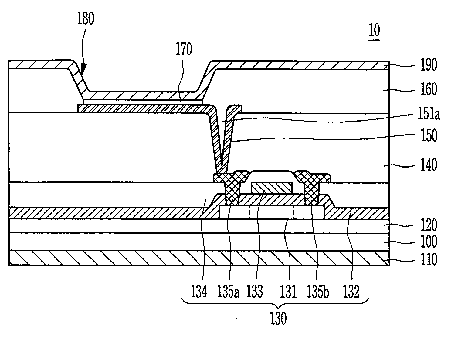
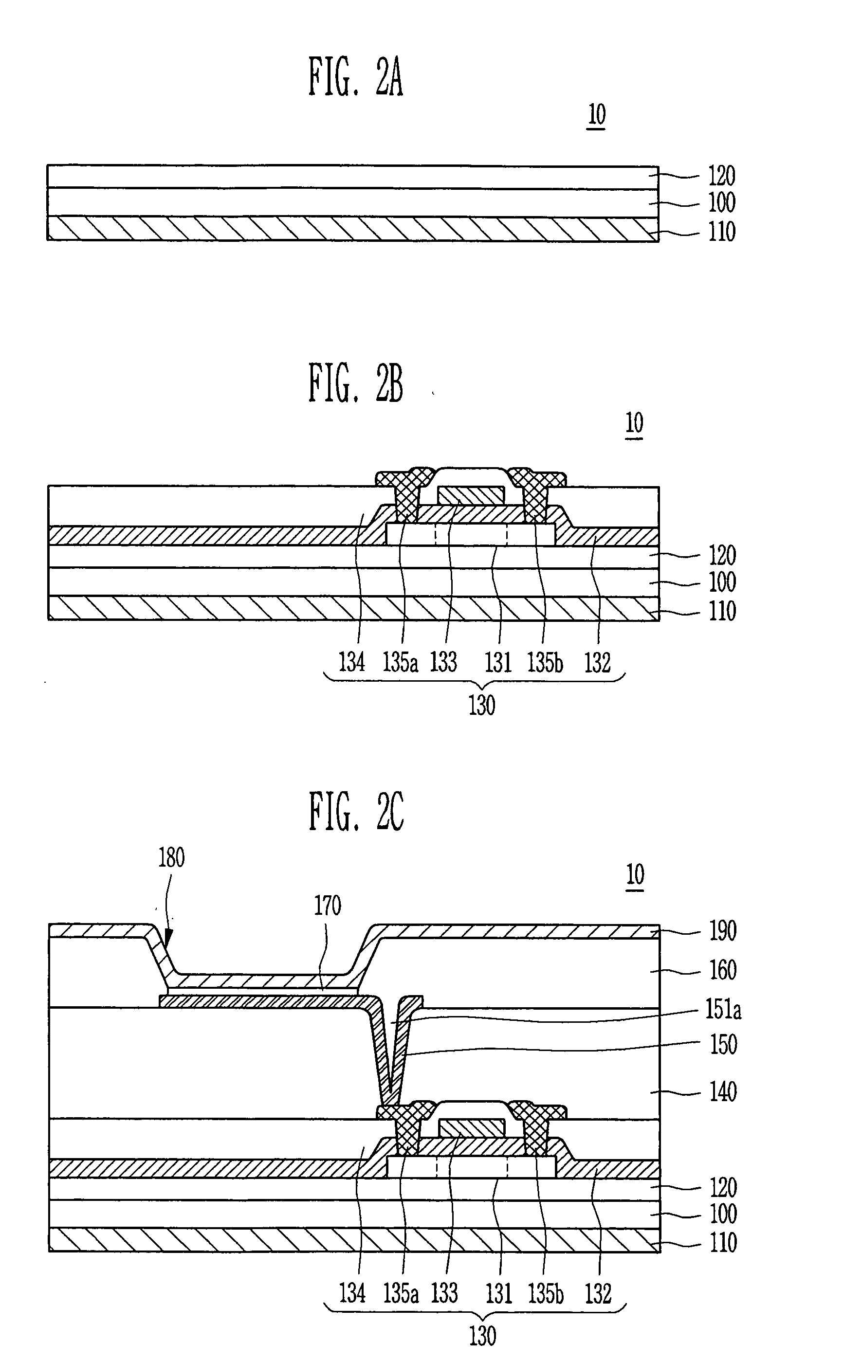
[0023]FIG. 1 is a schematic sectional view of an Organic Light Emitting Display (OLED) according to the present invention.

[0024] Referring to FIG. 1, an OLED 10 includes a transparent substrate 100, a photochromatic layer 110 formed on a first surface of the transparent substrate 100, at least one transparent Thin Film Transistor (TFT) 130 formed on a second surface of the transparent substrate 100, and an organic light emitting device formed on and electrically connected to the transparent TFT 130.

[0025] The transparent substrate 100 can be formed of an insulating material, such as glass, plastic, silicon, or a synthetic resin, and is preferably a transparent substrate, such as a glass substrate.

[0026] The photochromatic layer 110 is formed on a first surface of the transparent substrate 100 of at least one of an inorganic, an organic, or a glass material that visibly changes by light. In particular, the photochromatic layer 110 is preferably formed of a borosilicate containing A...

second embodiment

[0058]FIG. 3 is a schematic sectional view of an organic light emitting display according to the present invention.

[0059] Referring to FIG. 3, an OLED 20 includes a transparent substrate 200, a photochromatic layer 210 formed on a first surface of the transparent substrate 200, at least one transparent Thin Film Transistor (TFT) 230 formed on a second surface of the transparent substrate 200, and an organic light emitting device formed on and electrically connected to the transparent TFT 230.

[0060] The transparent substrate 200 can be formed of an insulating material, such as glass, plastic, silicon, or a synthetic resin, and is preferably a transparent substrate, such as a transparent glass substrate.

[0061] The photochromatic layer 210 is formed on a first surface of the transparent substrate 200 of at least one of inorganic, organic, and glass materials that visibly change by light. In particular, the photochromatic layer 210 is preferably formed of a borosilicate containing Ag ...


PUM


Abstract

An Organic Light Emitting Display (OLED) and its method of fabrication includes: a transparent substrate; a photochromatic layer formed on a first surface of the transparent substrate; at least one transparent Thin Film Transistor (TFT) formed on a first surface of the transparent substrate, and an organic light emitting device formed on and electrically connected to the transparent TFT.

Description

CLAIM OF PRIORITY [0001] This application makes reference to, incorporates the same herein, and claims all benefits accruing under 35 U.S.C. §119 from an application for ORGANIC LIGHT EMITTING DISPLAY AND FABRICATION METHOD FOR THE SAME earlier filed in the Korean Intellectual Property Office on the 28th of Jul. 2005 and there duly assigned Serial No.10-2005-0069173. BACKGROUND OF THE INVENTION [0002] 1. Field of the Invention [0003] The present invention relates to an Organic Light Emitting Display (OLED) and its method of fabrication, and more particularly, to an OLED and its method of fabrication in which a photochromatic layer is formed on a first surface of a transparent substrate of an OLED so that it is possible to realize a light emitting display of high visibility and contrast even when intense external light is incident. [0004] 2. Description of the Related Art [0005] An OLED is formed of uniform and flat thin films. Also, in the OLED, an electrode that emits light is form...

Claims


Application Information

Patent Timeline
IPC IPC(8): H01J1/62H01J63/04
CPCH01L27/3244H01L2251/5323H01L51/5281H10K59/12H10K50/86H10K2102/3031H05B33/22H05B33/10
Inventor SHIN, HYUN SOOJEONG, JAE KYEONGMO, YEON GONJIN, DONG UN
Owner SAMSUNG DISPLAY CO LTD
Why Eureka
Try Eureka