Light-collecting apparatus and contact-type solid-state imaging apparatus using the same

a light collection and imaging apparatus technology, applied in the field of contact-type solid-state imaging apparatus, can solve the problems of not having a difficult for imaging apparatus to implement downsizing and realize high resolution, and relatively longer lens diameter. , to achieve the effect of reliable modulation transfer function (mtf) characteristic, long lens diameter and high resolution

Inactive Publication Date: 2007-02-15
PANASONIC CORP
View PDF10 Cites 30 Cited by
  • Summary
  • Abstract
  • Description
  • Claims
  • Application Information

AI Technical Summary

Benefits of technology

[0010] As mentioned above, the current refractive index distribution rod lens has a relatively longer lens diameter and does not have a reliable Modulation Transfer Function (MTF) characteristic. Thus, it is not easy for the imaging apparatus to implement downsizing and to realize high resolution. Hence, it will be necessary to develop a new light-collecting device which is able to control a reflection index accurately comparing with a refractive index distribution rod lens, and also which can be formed easily in order to realize downsizing, lowering the cost, and high performance of a contact-type solid-state imaging apparatus.

Problems solved by technology

As mentioned above, the current refractive index distribution rod lens has a relatively longer lens diameter and does not have a reliable Modulation Transfer Function (MTF) characteristic.
Thus, it is not easy for the imaging apparatus to implement downsizing and to realize high resolution.

Method used


Image

  • Light-collecting apparatus and contact-type solid-state imaging apparatus using the same
  • Light-collecting apparatus and contact-type solid-state imaging apparatus using the same
  • Light-collecting apparatus and contact-type solid-state imaging apparatus using the same

Examples


first embodiment

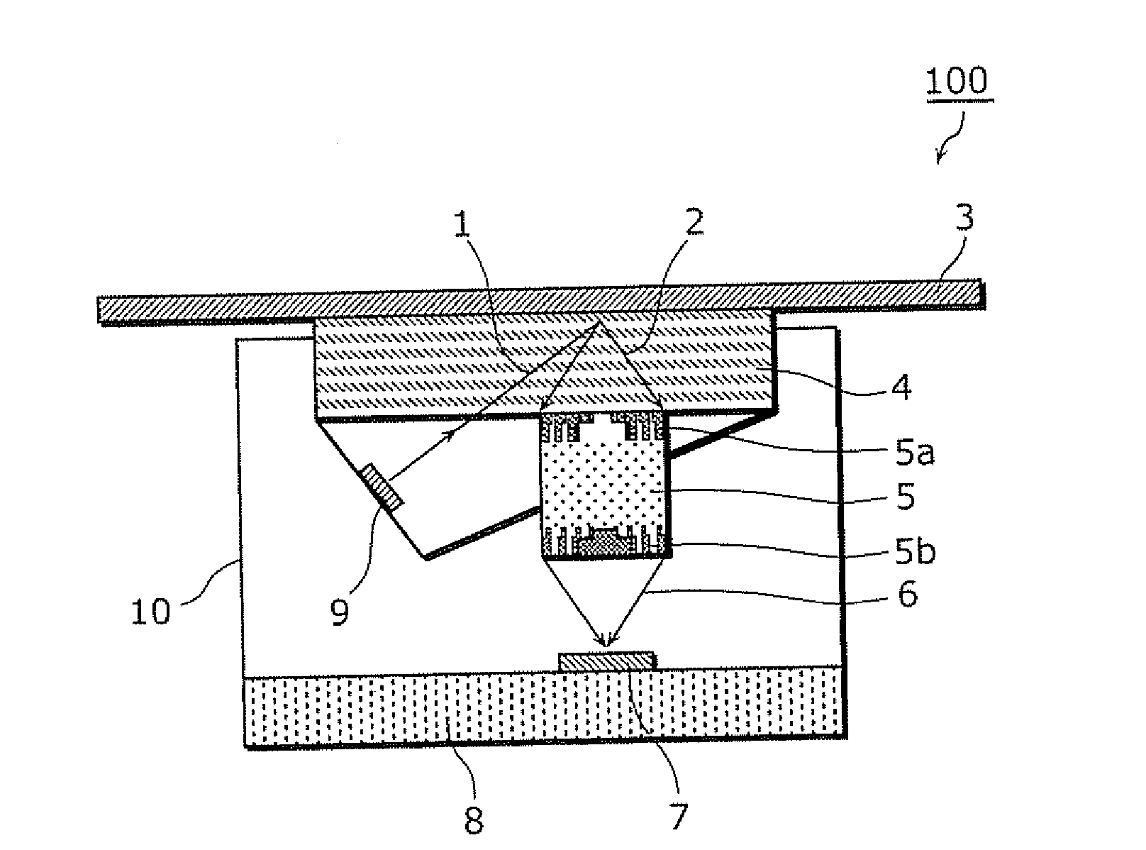
[0045]FIG. 5 is a diagram showing a contact-type solid-state imaging apparatus 100 which supports a resolution 600 dpi of the present embodiment. The contact-type solid-state imaging apparatus 100 in FIG. 5 is an example of a structure by pixel unit, and includes a protection glass plate 4, a light-collecting device 5, a light-receiving device 7, a semiconductor integrated circuit 8, a light emitting diode (LED) 9 and a mounting package 10.

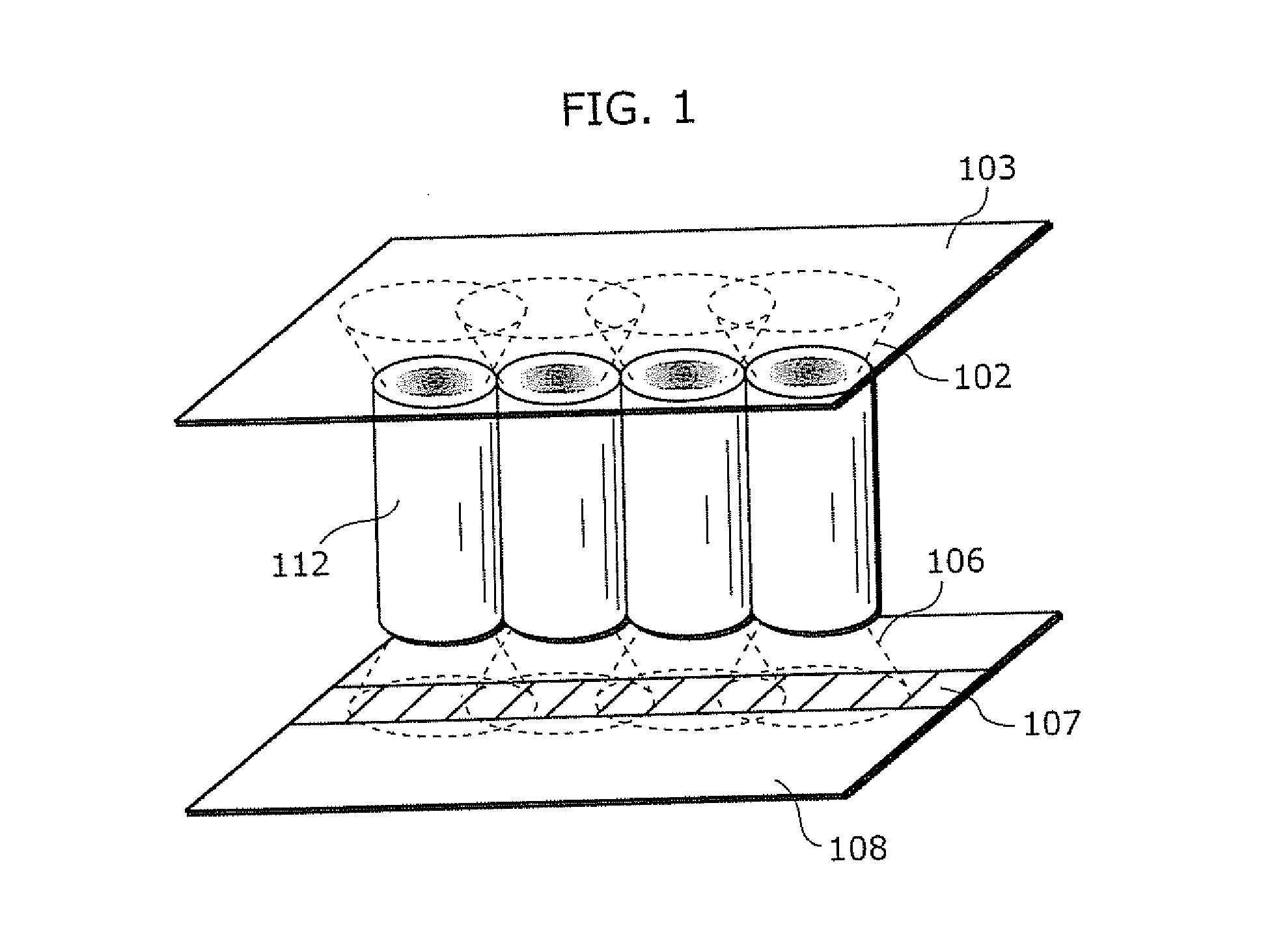
[0046] A light emitted from the LED 9 is diffused and reflected on the surface of the object (original copy) 3, and is collected at the light-receiving device 7 via the light-collecting device 5. At this timer the light-collecting device 5 has two distributed index lenses 5a and 5b.

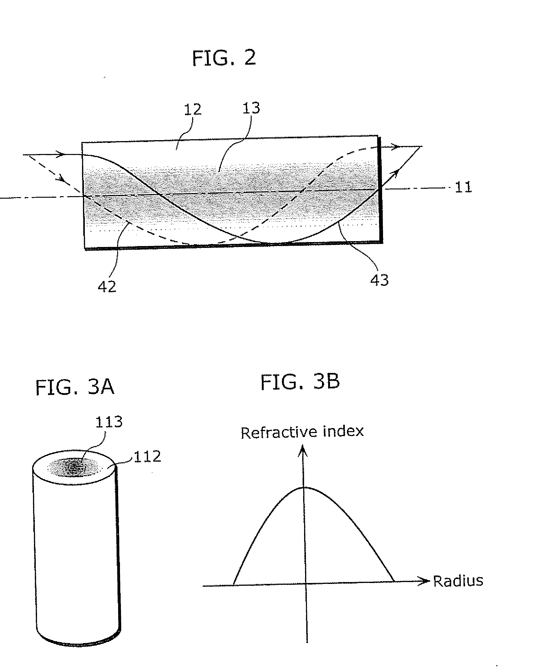
[0047]FIG. 6A is a cross-sectional diagram showing the distributed index lens with a concentric structure including SiO2 12 (refractive index=1.45) and SiN 13 (refractive index=2.0) of the present embodiment. The refractive index of such general distributed index lens...

second embodiment

[0061]FIG. 10 is a diagram showing the light-collecting apparatus in the contact-type solid-state imaging apparatus of a color scanner for a personal computer (300 dpi) and a pixel array of the second embodiment. A signal light 2 is collected by a light-collecting apparatus 27 structured by plural distributed index lens 26 arranged in two-dimensional array, and is irradiated onto a single light-receiving device 7. Here, the light-collecting apparatus 27 includes a lens group at incident light side 28 and a lens group at light outgoing side 29, and the each lens group has a light-collecting and a deflecting. In this state, as for an incident light which is incident vertical with respect to the in-plane direction of the light-collecting apparatus 27, the parameter θ of the aforesaid equation (1) is 0°. The concentric structure of the distributed index lens 26 is symmetrical with respect to the pixel center. However, when the incident angle is increased (θ component is increased), the ...

third embodiment

[0065]FIG. 13 is a diagram showing the light-collecting apparatus in the contact-type solid-state imaging apparatus of a color scanner for a personal computer (300 dpi) and a pixel array of the third embodiment. The signal light 2 is collected by the light-collecting apparatus 27 structured by plural distributed index lens 26, and is irradiated onto the single light-receiving device 7. Here, the light-collecting apparatus 27 includes a lens group at incident light side 28 and a lens group at light outgoing side 29. In this case, the incident light 2 is near-vertical with respect to the in-plane direction of the light-collecting apparatus, and thus the parameter θ of the aforesaid equation (1) is 0°. The concentric structure of the distributed index lens 26 is symmetrical with respect to the pixel center.

[0066] In the present embodiment, a line sensor of 300 dpi is used as an example. When the lens diameter of the distributed index lens is smaller, it is possible to correspond to fi...


PUM

PropertyMeasurementUnit
diameteraaaaaaaaaa
pixel sizeaaaaaaaaaa

Abstract

The present invention provides a contact-type solid-state imaging apparatus which realizes high resolution and high sensitivity, and also implements downsizing and lowering the cost of the contact-type solid-state imaging apparatus. Each pixel includes a protection glass plate, a light-collecting device, a light-receiving device, a semiconductor integrated circuit, a light emitting diode (LED) and a mounting package. The light-collecting apparatus has two kinds of distributed index lens (o lens and convex lens), and Sin (N=2) film, which is a two-stage concentric structure, is embedded in SiO2 (N=1.45) film.

Description

BACKGROUND OF THE INVENTION [0001] (1) Field of the Invention [0002] The present invention relates to a solid-state imaging apparatus, and particularly to a contact-type solid-state imaging apparatus and the like. [0003] (2) Description of the Related Art [0004] A solid-state imaging apparatus (image sensor) is an essential element of an image input apparatus used for various types of image areas including a digital video camera (DVC), a digital still camera (DSC) and the like. In recent years, along with a spread of paperless information, that is, computerized image and character database, an image scanner apparatus has been increasingly in demand. Thus, it has been greatly demanded for a contact-type solid-state imaging apparatus which is used for the image scanner apparatus to implement downsizing and to realize high resolution. [0005]FIG. 4 is a diagram showing a system structure of a conventional contact-type solid-state imaging apparatus. A light emitting diode 109 irradiates ...

Claims


Application Information

Patent Timeline
Patent Type & Authority Applications(United States)
IPC IPC(8): G01N21/00
CPCG02B3/0087G02B5/1876H04N1/0312H04N1/0282H04N1/0311G02B5/1885
Inventor TOSHIKIYO, KIMIAKIKOJIMA, MOTOHIROONOZAWA, KAZUTOSHI
Owner PANASONIC CORP
Why Eureka
Try Eureka