Domino logic testing systems and methods

US20070296465A1Inactive Publication Date: 2007-12-27UNIVERSITY OF MISSOURI

Image

  • Domino logic testing systems and methods
  • Domino logic testing systems and methods
  • Domino logic testing systems and methods

Examples


Embodiment Construction

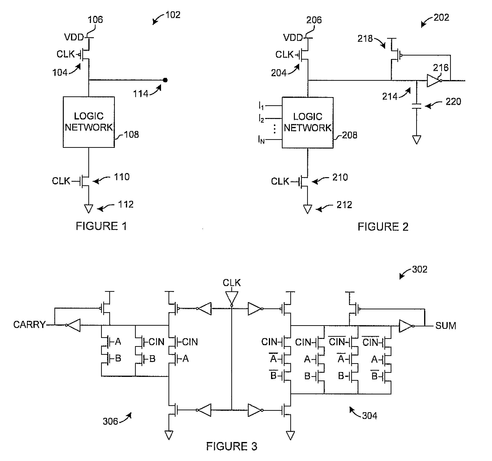
[0031]A fault dictionary of a CMOS domino logic circuit can be used to identify a fault model. In one example, a fault dictionary is determined using a CMOS domino logic full adder circuit. Although, other types of domino logic circuits may be used.

[0032]As depicted in the example of FIG. 3, a domino logic full adder 302 includes a domino logic circuit 304 to generate a sum output (S=A⊕B⊕Cin) and a domino logic circuit 306 to generate a carry output (Co=A.B+B.Cin+A.Cin). Faults occurring in the sum (S) and the carry output (Co) of the domino logic full adder 302 are then used to identify classes of faults for the circuit.

[0033]Faults are grouped for a fault model. In the example of FIG. 3, the faults include stuck-at-0 faults, stuck-at-1 faults, transistor stuck on / open faults, floating node faults, and bridging faults. Faults that occur under this fault model include faults that make the domino logic circuit appear fault free and do not cause any quiescent or static current (Iddq) ...


PUM


Abstract

A domino logic test circuit includes a dynamic node, a precharge device for charging the dynamic node, and an output inverter for inverting an output of the dynamic node. A logic network is coupled to the dynamic node for discharging the dynamic node in accordance with logic. A footer device enables and disables the logic network. A keeper device is coupled to the dynamic node for retaining a charge state of the dynamic node while awaiting the logic network to operate in accordance with the logic. A test mode selection device is coupled to the dynamic node and is configured to enable a latch in the test mode. A phase selection device is configured to receive at least a wait signal and to enable selection of at least a precharge phase for charging the dynamic node to a voltage level, a write phase for generating a value to the latch based on the logic and the voltage level of the dynamic node, and a wait phase for enabling reading the value. The selection is based, at least partially, on the wait signal state.

Description

RELATED APPLICATIONS[0001]Not ApplicableFEDERALLY SPONSORED RESEARCH OR DEVELOPMENT[0002]Not ApplicableCOMPACT DISK APPENDIX[0003]Not ApplicableBACKGROUND OF THE INVENTION[0004]Dynamic logic circuits have become prevalent in high performance integrated circuits because they offer faster switching speeds and a smaller area than static logic circuits. Dynamic logic circuits generally use complementary metal oxide semiconductor (CMOS) devices.[0005]As depicted in FIG. 1, a dynamic logic circuit 102 includes a p-type channel MOS (PMOS) precharge transistor 104 coupled to a voltage source 106 having a voltage level (Vdd), an n-type channel MOS (NMOS) logic network 108, and an NMOS footer transistor 110 coupled to ground 112. The output is measured at a dynamic node 114. The circuit operation is controlled by a clock signal (CLK) that is applied to both the PMOS precharge transistor 104 and the NMOS footer transistor 110.[0006]The dynamic logic circuit 102 has two phases of operation. Whe...

Claims


Application Information

Patent Timeline
27 Dec 2007
Publication
US20070296465A1
IPC
H03K19/096
CPC
G01R31/317
Inventors
AL-ASSADI, WALEED K.; CHANDRASEKHAR, PAVANKUMAR