

Method for fabricating embedded static random access memory
- Summary
- Abstract
- Description
- Claims
- Application Information
AI Technical Summary
Benefits of technology
Problems solved by technology
Method used
Image

Examples
Embodiment Construction
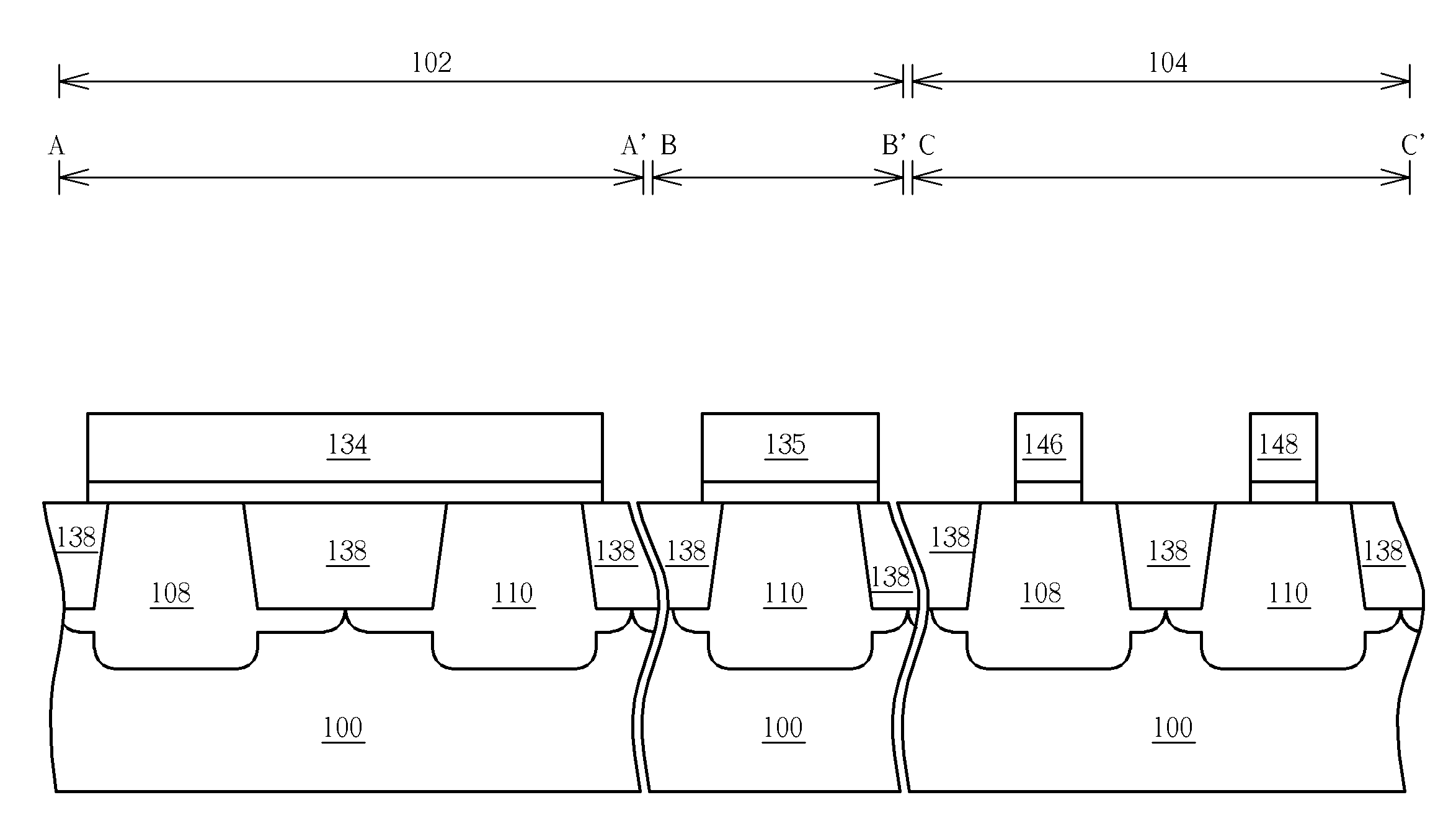
[0028]Please refer to FIG. 3, which shows a schematic plan view of an embedded static ransom access memory in accordance with the present invention. A semiconductor substrate 100 is provided. A memory cell area 102 and a logic area 104 are defined on the semiconductor substrate 100. According to different designs and functional desires for the electrical circuits, a plurality of active areas 106, N wells 108 and P wells 110 are formed respectively in the memory cell area 102 and the logic area 104 of the semiconductor substrate 100. Therefore, P type conductive devices are formed on the N well 108 and N type conductive devices are formed on the P well 110. The N well 108 may comprise a plurality of P type conductive device areas, on which a P type conductive device is formed. Equally, the P well 110 may comprise a plurality of N type conductive device areas, on which an N type conductive device is formed. Subsequently, a patterned silicon layer 112 is deposited on the N well 108, th...
PUM
 Abstract
Description
Claims
Application Information