

Low distortion high bandwidth adaptive transmission line for integrated photonic applications
a photonic application, low distortion technology, applied in waveguides, optical radiation measurement, instruments, etc., can solve the problems of difficult to achieve a final, difficult to maximize the impedance and velocity of unloaded transmission lines, and insufficient space utilization of modulators
- Summary
- Abstract
- Description
- Claims
- Application Information
AI Technical Summary
Benefits of technology
Problems solved by technology
Method used
Image

Examples
Embodiment Construction
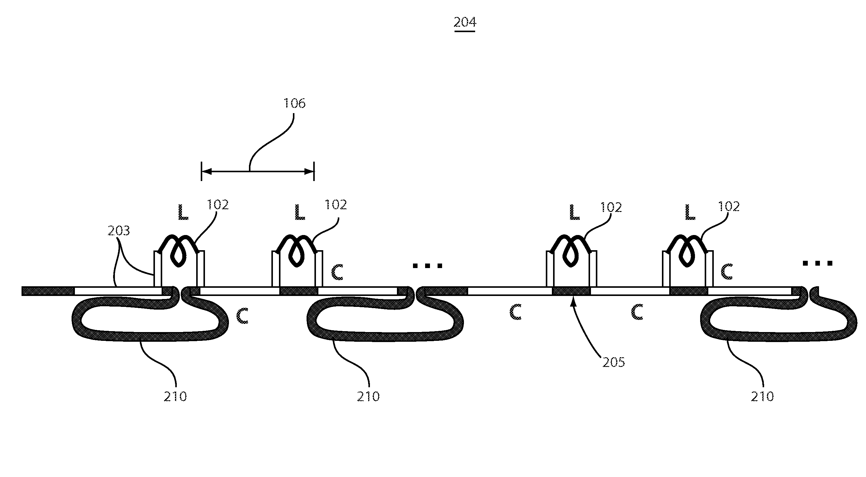
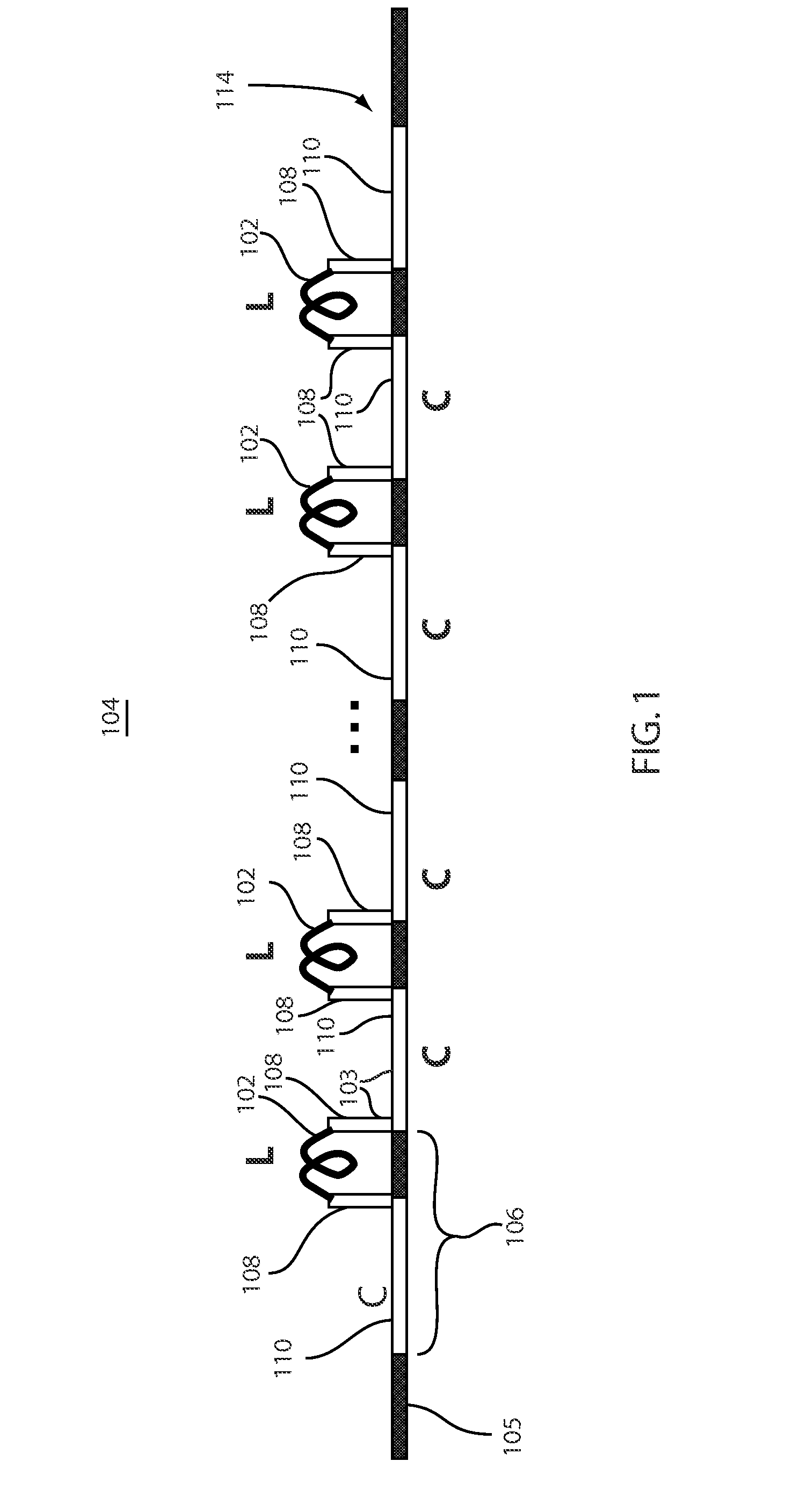
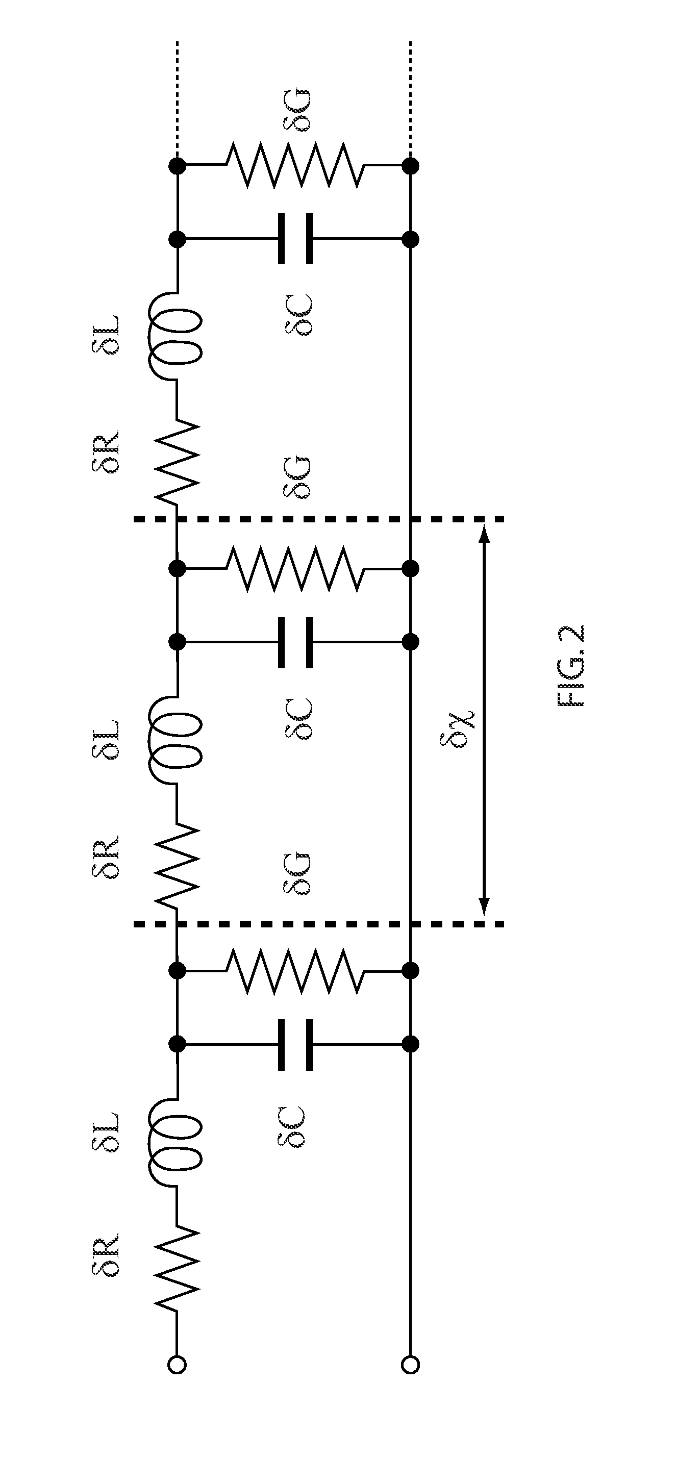
[0021]In accordance with the present principles, an optimized traveling wave (TW) structure and control circuit for semiconductor optical modulators is provided. In a particularly useful embodiment, photonic modulators are fabricated in an integrated circuit process (e.g., a complementary metal oxide semiconductor (CMOS) process) with multiple metal layers. Aspects of the present systems and methods include: distributed electrodes utilizing multi-metal layer inductors to balance optical modulator capacitance to achieve a desired characteristic impedance; low-loss optical delay lines inserted between active modulator segments to slow down the optical wave being modulated and match its velocity to the electrical modulating signal; and a tunable control circuit and method for implementing the tunable control circuit for velocity matching the electrical modulation signal and optical signal traveling in a transmission line (e.g., of an optical modulator).
[0022]Aspects of the present inve...
PUM
 Abstract
Description
Claims
Application Information