Method, controller, and memory device for correcting data bit(s) of at least one cell of flash memory

US20130332801A1Active Publication Date: 2013-12-12SILICON MOTION INC (TW)
5 Cites 14 Cited by

Patent Information

Authority / Receiving Office
US · United States
Current Assignee / Owner
Publication Date
2013-12-12

Smart Images

  • Figure 1
    Figure 1
  • Figure 2
    Figure 2
  • Figure 3
    Figure 3
Patent Text Reader

Abstract

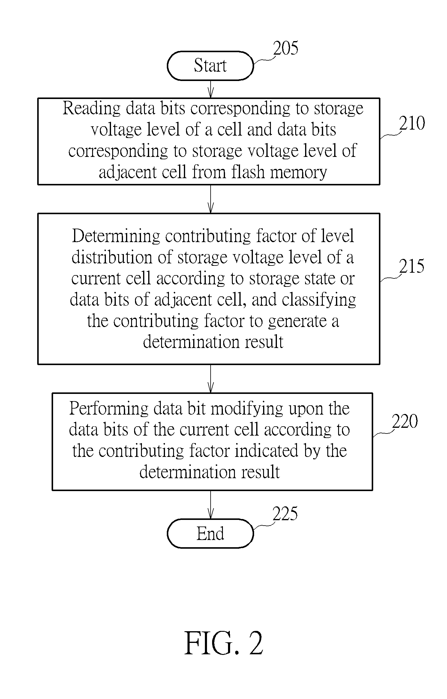
A method for correcting data bit of at least a cell of a flash memory includes: determining a contributing factor of level distribution corresponding to an electric level of a first cell to generate a first determination result; and, correcting / modifying the data bit corresponding to the electric potential of the first cell according to the first determination result.
Need to check novelty before this filing date? Find Prior Art

Description

CROSS REFERENCE TO RELATED APPLICATIONS

[0001] This application claims the benefit of U.S. Provisional Application No. 61 / 657,035 filed on Jun. 8, 2012, which is entirely incorporated herein by reference.BACKGROUND OF THE INVENTION

[0002] 1. Field of the Invention

[0003] The present invention relates to a data correction scheme for a flash memory, and more particularly to a method, controller, and a memory device for correcting data bit(s) of at least one cell of the flash memory.

[0004] 2. Description of the Prior Art

[0005] Generally speaking, an error correction code (ECC) processing circuit may be configured within a conventional flash memory controller. The conventional flash memory controller uses the ECC processing circuit to try to correct data bits read out from a flash memory so as to try to obtain correct data bits. When the total bit errors of codeword data can still corrected by the conventional ECC processing circuit, this indicates that the conventional ECC processing circuit i...

Examples

Embodiment Construction

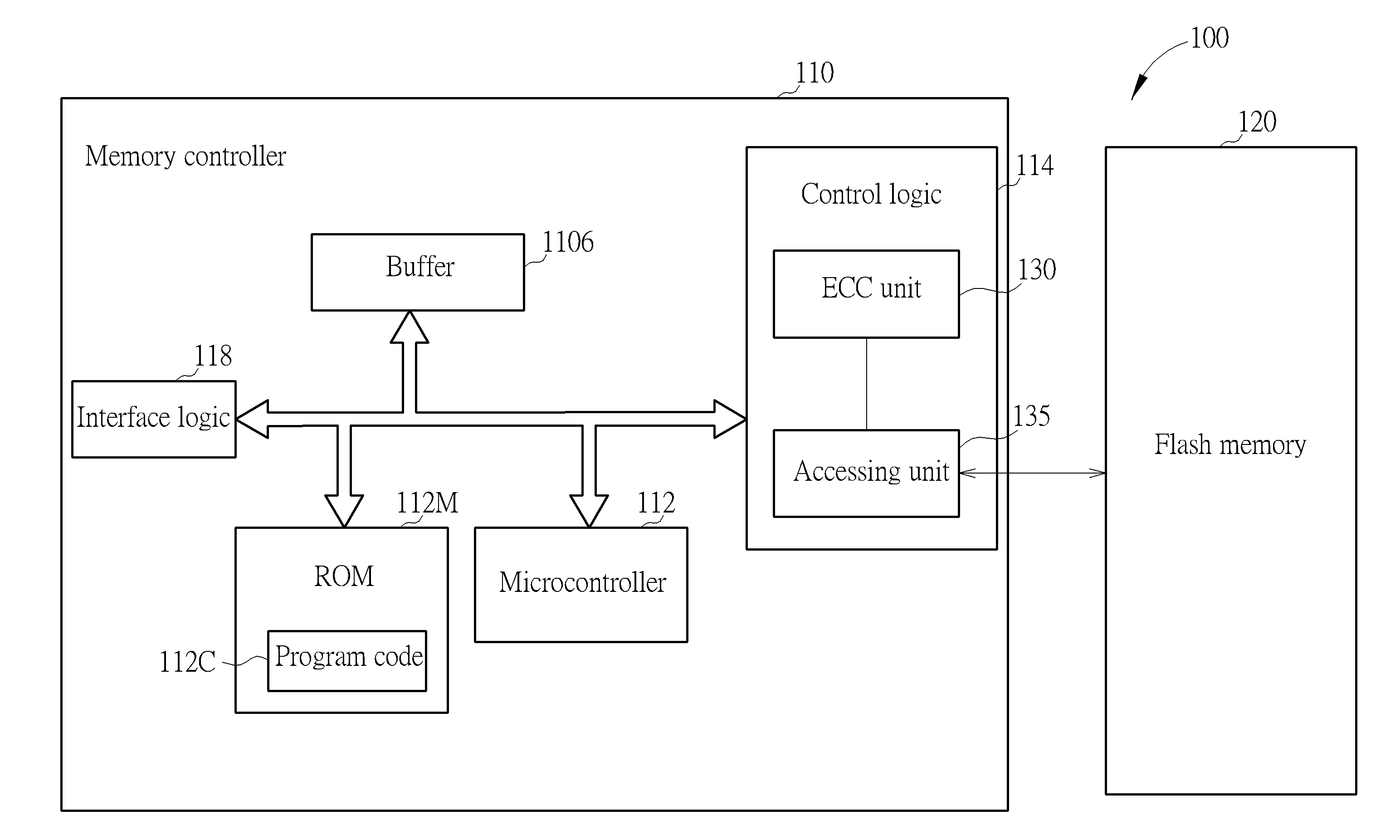
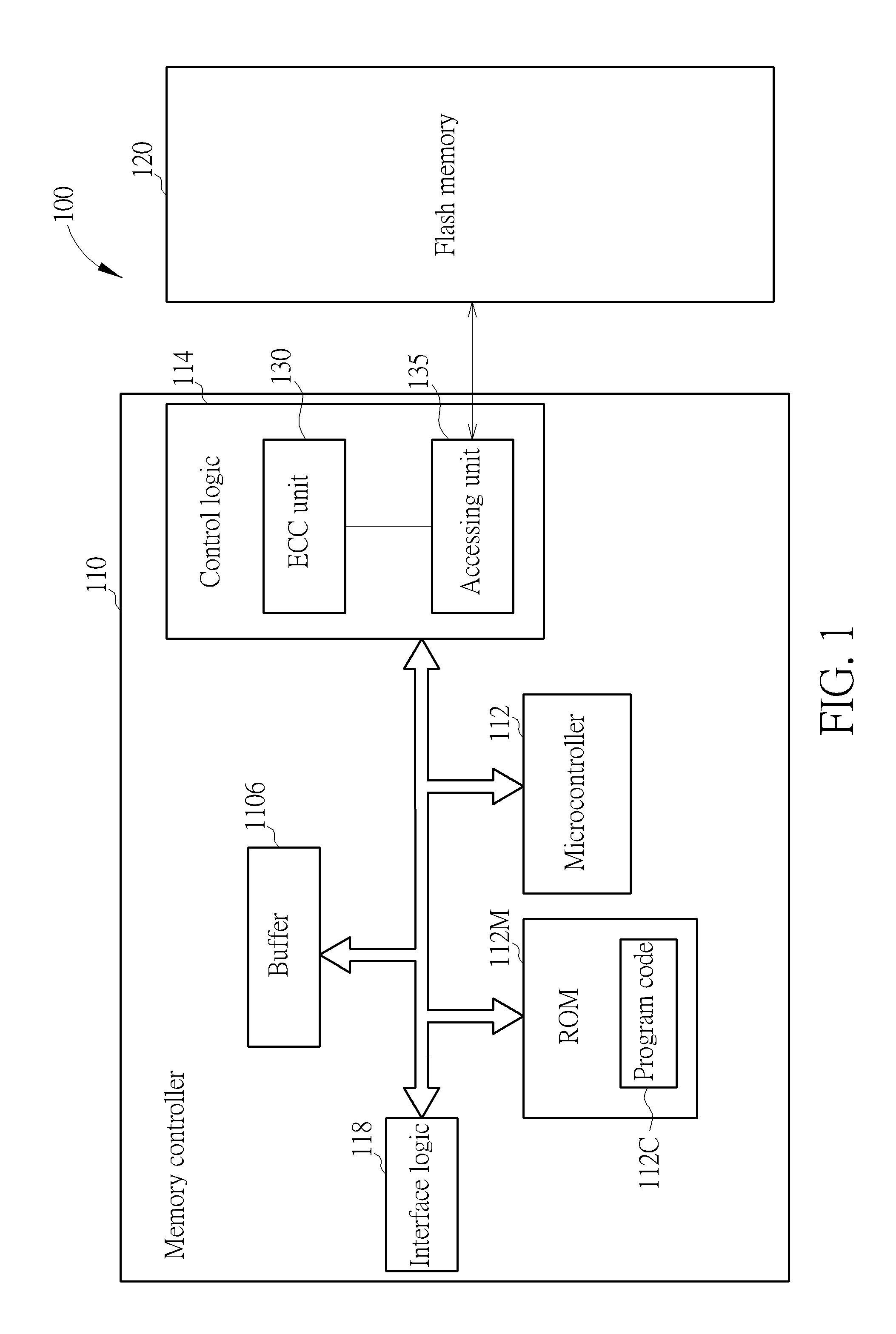
[0019]Please refer to FIG. 1, which is a diagram of a memory device 100 according to an embodiment of the present invention. In this embodiment, the memory device 100 is implemented by a portable memory device such as a memory card that satisfies one of different standards SD / MMC, CF, MS, and XD. The memory device 100 comprises a flash memory 120 and a controller. The controller can be a memory controller 110 and utilized for accessing the flash memory 120. According to this embodiment, the memory controller 110 comprises a microcontroller 112, a read-only-memory (ROM) 112M, a control logic 114, a buffer 116, and an interface logic 118. The ROM 112M is utilized for storing a program code 112C. The microcontroller 112 is arranged to execute the program code 112C for controlling the data access of the flash memory 120. In addition, the control logic 114 comprises an error correction code (ECC) unit 130. The flash memory 120 comprises a plurality of blocks, and the memory controller 11...