

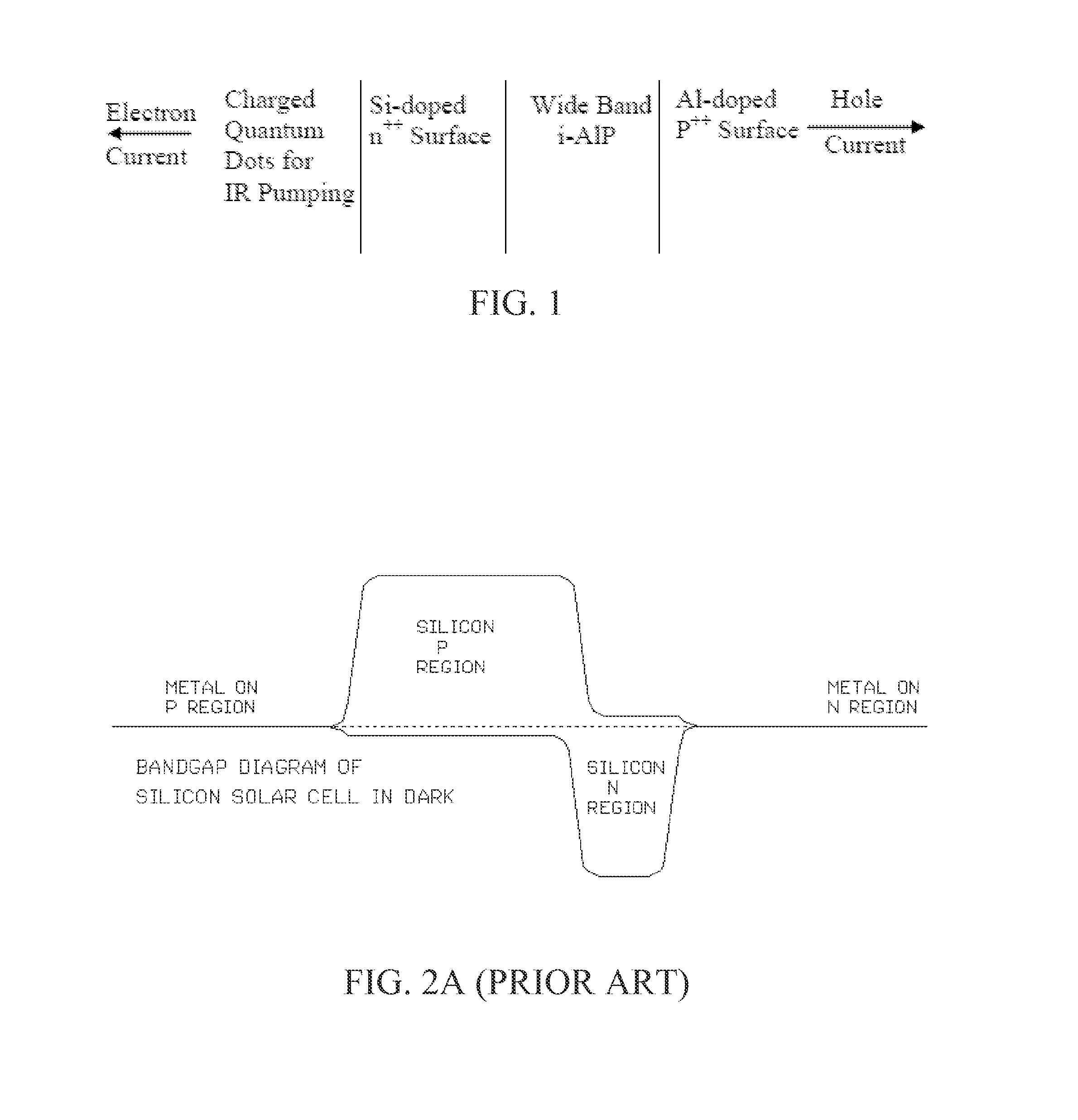
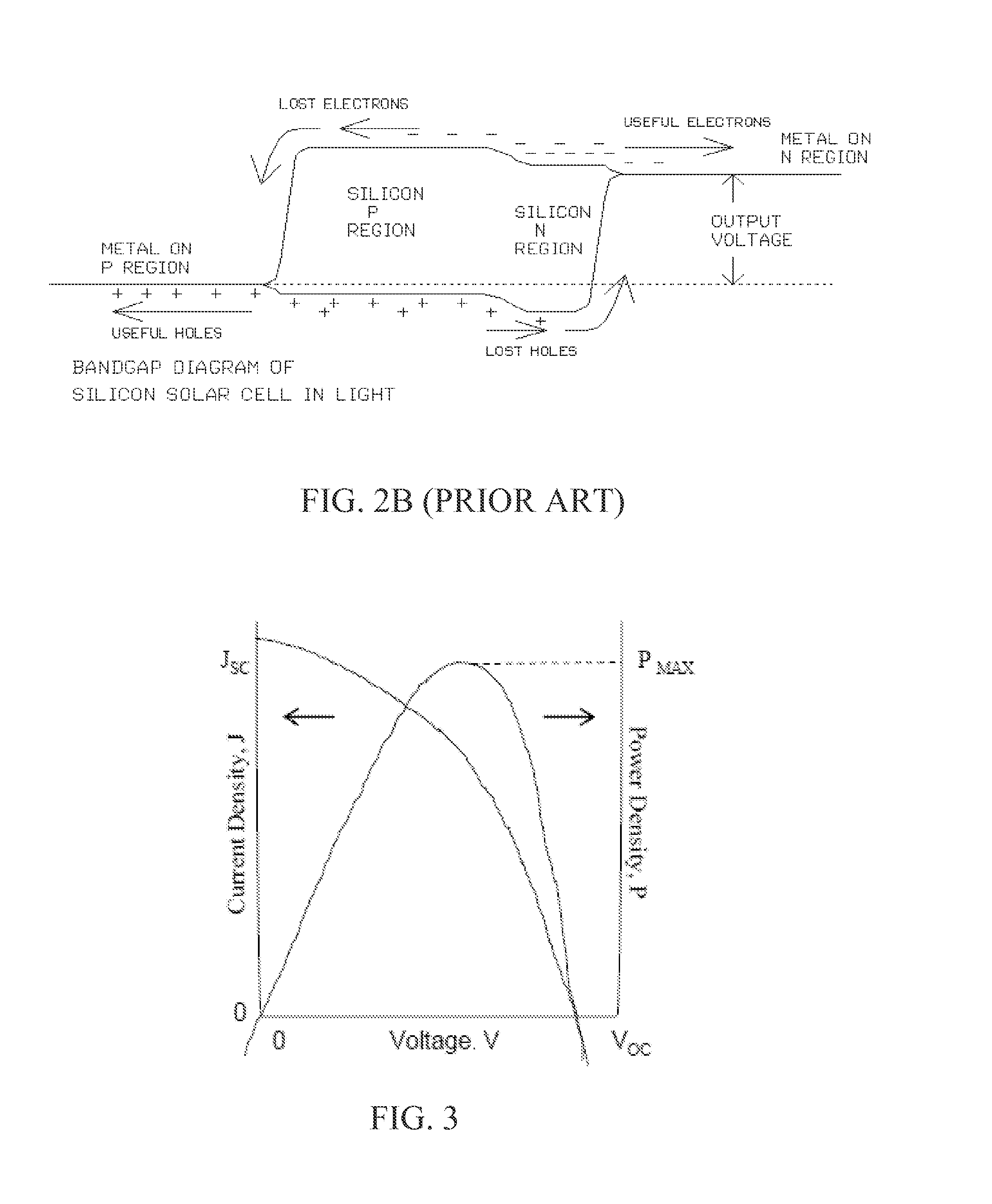
High efficiency solar cells with quantum dots for ir pumping
a solar cell and quantum technology, applied in the field of high efficiency solar cells with quantum dots for ir pumping, can solve the problems of notoriously difficult fabrication and integration of pv devices, reducing unit fabrication cost and unit facility cost, and achieving the effect of increasing material and fabrication facility costs and high efficiency
- Summary
- Abstract
- Description
- Claims
- Application Information
AI Technical Summary
Benefits of technology
Problems solved by technology
Method used
Image

Examples
examples
[0068]The following tasks may be carried out to form and evaluate a solar cell in accordance with the invention described herein.
Task 1. Fabrication of Monocrystalline Si PV Cells
[0069]200 mm p-Si wafer at 40-60μ with Boron dopant can be covered with one μ of n+ Si layer by PECVD with phosphorus dopant and annealed with H2 gas at 900° C. to form an epi-Si PV cell.
Task 2. Formation of n++ AlP / p++-Si
[0070]Al foil at 4 μ thick can be placed on the 200 mm p-Si wafer surface and placed in an oven with P vapor at 300° C. to form the self-liming i-AlP. The remaining Al from the self-limiting i-AlP will merge into the p-Si at an elevated temperature beyond 660° C. and become an additional p-dopant for the p-Si to form p++-Si surface, and shallowly implanting Si on i-AlP to replace Al in AlP becoming the n-dopant for the n++-AlP surface.
Task 3. Simulated Solar Radiation Spectrum and PV Efficiency Evaluations
[0071]A commercial light source of stimulated solar radiation spectrum can be used a...
PUM
 Abstract
Description
Claims
Application Information