

Light-emitting device
a technology of light-emitting devices and led devices, which is applied in the direction of semiconductor devices, basic electric elements, electrical equipment, etc., can solve the problems of adverse influence on the light-emitting of led devices
- Summary
- Abstract
- Description
- Claims
- Application Information
AI Technical Summary
Problems solved by technology
Method used
Image


Examples
first embodiment
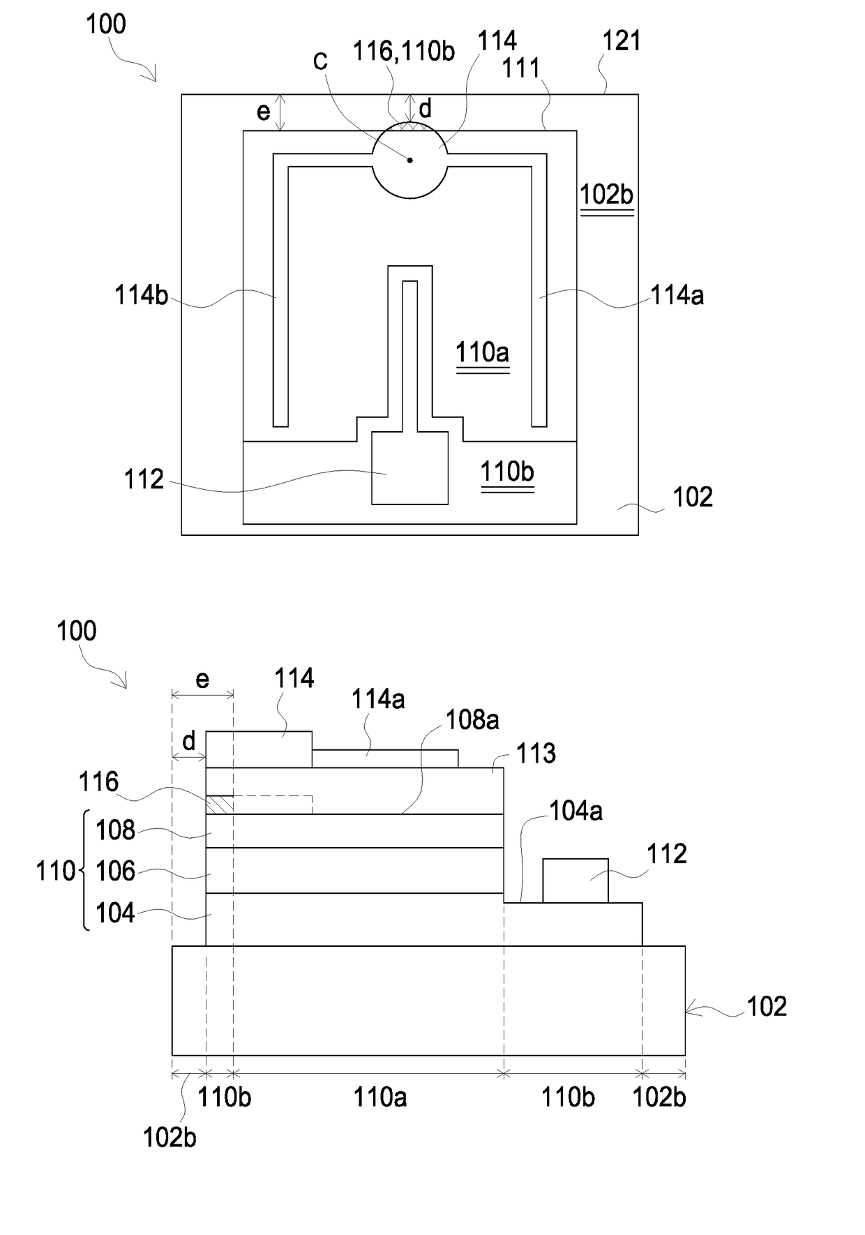
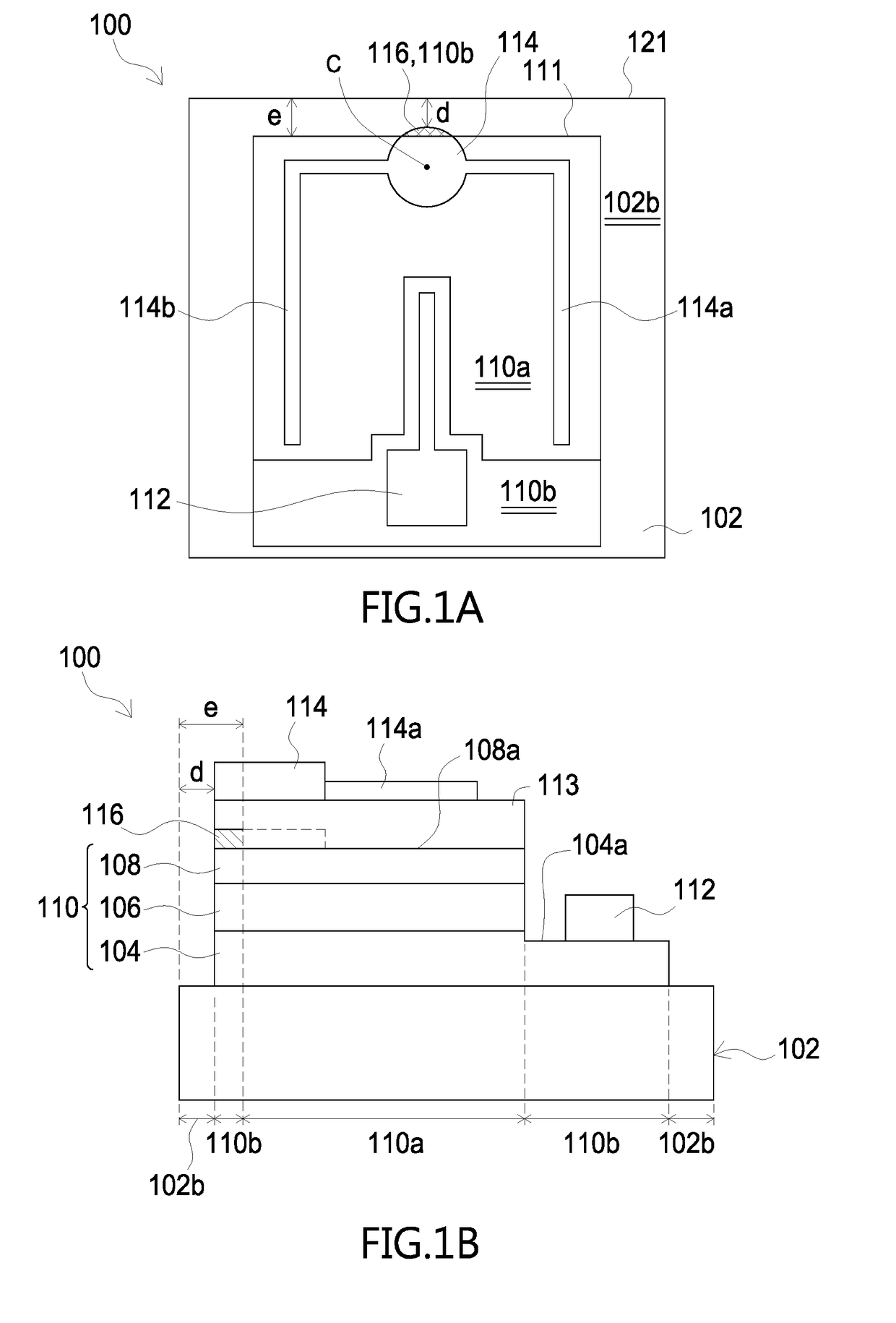
[0013]Referring to FIGS. 1A and 1B, a light-emitting device in accordance with the present application is disclosed. A light-emitting device 100 includes: a substrate 102, for example, an insulative and single-crystalline substrate, and in the embodiment the substrate 102 can be Sapphire; a light-emitting structure 110 formed on the substrate 102, including a lower semiconductor layer 104, an active layer 106 and an upper semiconductor layer 108; a first electrode 114 electrically connected to the upper semiconductor layer 108; and a second electrode 112 formed on the lower semiconductor layer 104. There are two portions defined in the light-emitting structure 110: a first portion 110a having a first top face 108a and a second portion 110b where no optoelectronic conversion occurs therein. The first portion 110a includes part of the upper semiconductor layer 108 having the first top face 108a, the active layer 106, and the lower semiconductor layer 104. In the embodiment, the ratio ...
second embodiment
[0018]Referring to FIGS. 2A and 2B, a light-emitting device 200 in accordance with the present application is disclosed. A light-emitting device 200 includes: a substrate 202, for example, an insulative and single-crystalline substrate, and in the embodiment the substrate 202 can be Sapphire; a light-emitting structure 210 formed on the substrate 202 including a lower semiconductor layer 204, an active layer 206 and an upper semiconductor layer 208; a first electrode 214 electrically connected to the upper semiconductor layer 208; and a second electrode 212 formed on the lower semiconductor layer 204. There are two portions defined in the light-emitting structure 210: a first portion 210a having a first top face 208a and a second portion 210b where no optoelectronic conversion occurs therein, having a second top face 204a lower than the first top face 208a. The first portion 210a includes part of the upper semiconductor layer 208 having the first top face 208a, the active layer 206,...
third embodiment
[0021]Referring to FIG. 3, a light-emitting device 300 in accordance with the present application is disclosed. A light-emitting device 300 includes: a substrate 302, for example, an insulative and single-crystalline substrate, and in the embodiment the substrate 302 can be Sapphire; a light-emitting structure 310 formed on the substrate 302, including a lower semiconductor layer 304, an active layer 306, and an upper semiconductor layer 308; a first electrode 314 electrically connected to the upper semiconductor layer 308; and a second electrode 312 formed on the lower semiconductor layer 304. There are two portions defined in the light-emitting structure 310: a first portion 310a having a first top face 308a and a second portion 310b where no optoelectronic conversion occurs therein. The second portion 310b has a second top face 304a lower than the first top face 308a. The first portion 310a includes the upper semiconductor layer 308 having part of the first top face 308a, the act...
PUM
 Abstract
Description
Claims
Application Information