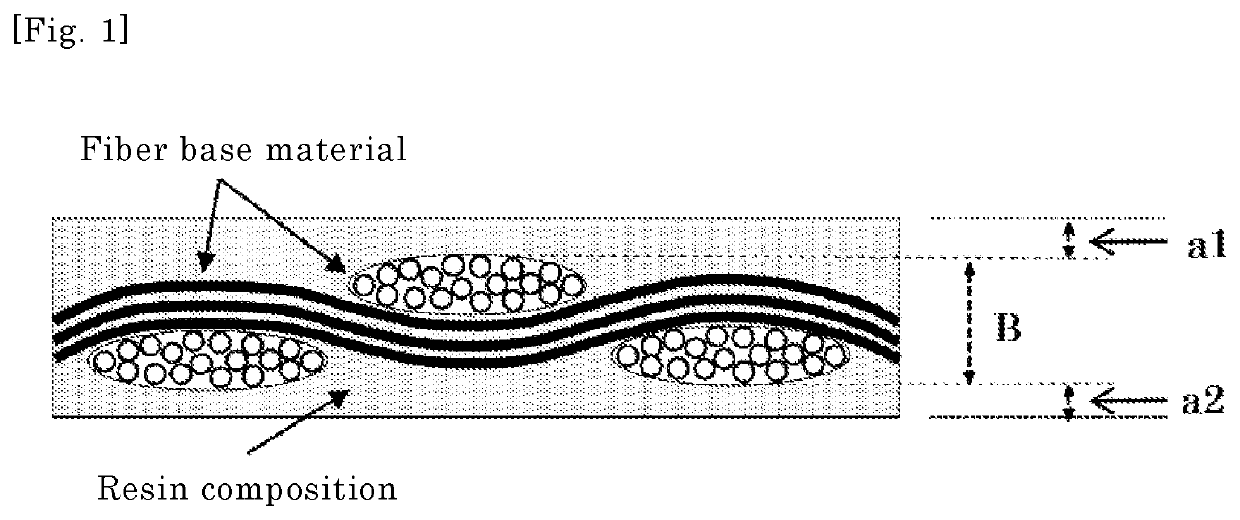
Metal-clad laminate, printed wiring board and semiconductor package
a technology of metal-clad laminates and printed circuit boards, which is applied in the direction of synthetic resin layered products, chemistry apparatuses and processes, other domestic articles, etc., can solve the problems of serious warping of printed circuit boards during the time of mounting thereof, and achieve the effect of suppressing warps
- Summary
- Abstract
- Description
- Claims
- Application Information
AI Technical Summary
Benefits of technology
Problems solved by technology
Method used
Image

Examples
example 1
(Subtractive Process)
[0118]With the procedure described below, the prepreg A and the copper-clad laminate were prepared.
(1. Preparation of Resin Varnish A)
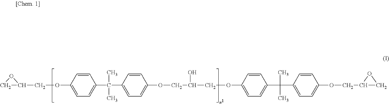
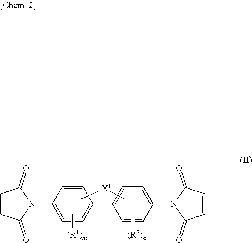
[0119]Into a vessel were taken 35.8 g of o-tolidine, 469.5 g of bis(4-maleimidephenyl)methane, 35.7 g of m-aminophenol, and 360.0 g of dimethylacetamide; and then, they were caused to react at 100° C. for 2 hours to obtain the polyimide compound-containing solution A (solid component concentration of 60% by mass), wherein the polyimide compound has a biphenyl skeleton in its molecular formula.
[0120]Into 50 parts by mass of the above-obtained polyimide compound-containing solution A (solid component concentration of 60% by mass) were added 30 parts by mass of the phenol novolak epoxy resin (trade name: EPICLON (registered trade mark) N-770″, manufactured by DIC Corp., epoxy equivalent of 188 g / eq), 20 parts by mass of the cresol novolak resin (trade name: PHENOLITE (registered trade mark) KA-1165, manufactured by Die Corp., hydroxy...
example 2
(Semi-Additive Process)
[0126]A sheet of the prepreg A obtained in Example 1 was cut to the size of 530 mm square; and this was interposed between two SAP-corresponding copper foils for the fine circuit having the size of 540 mum square (trade name: PF-EL5, which is the copper foil having a 4-μm thickness resin layer including an epoxy resin; manufactured by Hitachi Chemical Co., Ltd.) such that the resin layer sides thereof were facing to the prepreg A.
[0127]Next, this was interposed between the SUS-made mirror plates having the thickness of 1.8 mm and the size of 530 mm square, and heated under a vacuum atmosphere at the temperature raising rate of 2 to 3° C. / min in the product temperature range of 60 to 160° C. with the product pressure of 2.5 MPa; and then, this was kept at the maximum holding temperature of 220° C. for 90 minutes to obtain the laminate attached with the SAP-corresponding resin layer.
[0128]The copper foil in the outer layer of the laminate attached with the SAP-c...
example 3
[0129]The resin varnish A was prepared in the same way as Example 1.
[0130]The resin varnish A thus obtained was applied onto the PET film having the width of 580 mm (trade name: G-2, manufactured by Teijin DuPont Films Japan Ltd.) to obtain the resin film C by controlling the application in such a way that the width thereof would become 525 mm with the thickness of 50 μm after being dried. The temperature showing the lowest melt viscosity of this resin film was 121° C.
[0131]This was laminated to the glass woven cloth (thickness: 88 μm, weight: 104 g / m2, IPC #2116, base material's width: 530 mm, manufactured by Nitto Boseki Co., Ltd.), the fiber base material, in the same way as Example 1 to prepare the prepreg C.
[0132]One sheet of the prepreg C thus obtained was processed in the same way as Example 1 except that the temperature raising rate in the product temperature range of 60 to 160° C. was changed to 1.0 to 1.5° C. / min to prepare the copper-clad laminate C. The measurement resul...
PUM
| Property | Measurement | Unit |
|---|---|---|
| thickness | aaaaa | aaaaa |
| temperature | aaaaa | aaaaa |
| thickness | aaaaa | aaaaa |
Abstract
Description
Claims
Application Information
 - R&D
- Intellectual Property
- Life Sciences
- Materials
- Tech Scout
- Unparalleled Data Quality
- Higher Quality Content
- 60% Fewer Hallucinations
Browse by: Latest US Patents, China's latest patents, Technical Efficacy Thesaurus, Application Domain, Technology Topic, Popular Technical Reports.
© 2025 PatSnap. All rights reserved.Legal|Privacy policy|Modern Slavery Act Transparency Statement|Sitemap|About US| Contact US: help@patsnap.com